Overview
The Xiaomi Redmi Note 13 Pro is a mid-range smartphone featuring a Snapdragon 7 Gen 1 processor. Test points provide direct access to the device's eMMC storage and boot circuitry, enabling technicians to perform firmware flashing, FRP (Factory Reset Protection) removal, and recovery from soft-brick conditions. Understanding test point locations and proper connection procedures is essential for efficient device repair without factory reset complications.
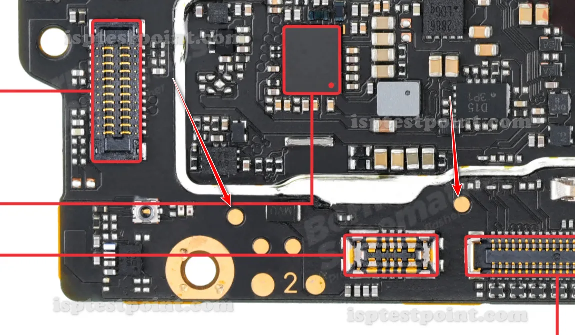
Test points on the Redmi Note 13 Pro are typically located on the main logic board near the eMMC chip. These pads allow ISP (In-System Programming) connection through specialized hardware tools, bypassing software-level security measures when necessary.

When to Use Test Points
Test points are required in the following scenarios:
- FRP (Google Account) lock removal without triggering additional verification
- Firmware flashing when device is soft-bricked or stuck in boot loops
- Complete dead-boot recovery when standard recovery mode is inaccessible
- IMEI repair and restoration procedures
- Emergency ROM restoration when OTA updates fail
Locating Test Points
The primary eMMC test points on the Redmi Note 13 Pro are situated on the rear side of the main PCB, typically in proximity to the eMMC storage chip. The exact coordinates and pad layout require careful visual inspection under magnification due to their small size (usually 0.5–1.5mm diameter).
Standard eMMC ISP pinout includes CLK, CMD, DAT0, DAT1, DAT2, DAT3, VCC, GND, and VCCQ lines. However, specific pad locations on this device model may vary by manufacturing batch. Technicians should verify pad positions using a high-resolution reference image or magnifying equipment before attempting connection.
Access Procedure
Begin by powering off the device completely. Carefully remove the protective layers and locate the test points using a microscope or magnifying lens. Use fine-tipped tweezers or precision probes to establish contact with each pad. Connect your ISP programmer (such as UMT or EasyJTAG Plus) according to your chosen tool's pinout requirements. Apply minimal pressure to avoid damaging the pads or surrounding components. Once connected, initiate the firmware operation through your programming software. Maintain stable contact throughout the entire process; intermittent connection may cause incomplete writes.
Safety Precautions
Always wear an anti-static wrist strap to prevent ESD damage to sensitive components. Do not exceed recommended voltage levels for your programming tool. Allow adequate cooling time between consecutive operations if performing multiple repairs. Never apply test points while the device is powered on or connected to USB. Handle the logic board with extreme care, as test point pads are easily damaged by mechanical stress or overheating. If uncertain about pad identification, consult high-resolution reference materials or seek guidance from experienced technicians before proceeding.
Pin / Test Point Reference
| Pin | Description |
|---|---|
| CLK | eMMC clock signal |
| CMD | eMMC command line |
| DAT0 | eMMC data line 0 |
| DAT1 | eMMC data line 1 |
| DAT2 | eMMC data line 2 |
| DAT3 | eMMC data line 3 |
| VCC | Primary power supply (typically 3.3V) |
| GND | Ground reference |
| VCCQ | I/O power supply |
Tools required: UMT (Universal Multi Tool), EasyJTAG Plus, ISP eMMC programmer, Fine-tipped precision probes, Anti-static wrist strap, Magnifying lens or USB microscope, Fine-tipped tweezers
Supported operations: Read Firmware, Write Firmware, FRP Erase, Dead Boot Repair, IMEI Restoration, Emergency ROM Flash
⚠ Safety note: High ESD risk. Use anti-static protection. Do not exceed 3.6V on eMMC pins. Maintain stable probe contact to avoid data corruption. Do not apply test points with device powered on.

Comments (0)
Be the first to comment.