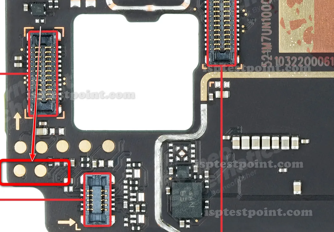
Redmi Note 12 Test Points — Overview of Hardware Diagnostic Access Locations
The Redmi Note 12 features multiple test points strategically located on the mainboard for direct hardware access during repair and unlock procedures. These pads enable technicians to bypass software locks, restore corrupted firmware, and diagnose power delivery failures. Test points are typically identified as small copper pads near the CPU, eMMC storage, and power management circuits. Accessing these points requires precision micro-probing equipment and steady hand technique to avoid damaging surrounding components.

When to Use Test Points — Troubleshooting Scenarios Requiring Direct Hardware Probing
Test point access is necessary when the device exhibits critical failures: FRP (Factory Reset Protection) lock preventing activation after owner reset, corrupted bootloader preventing normal boot sequence, deep discharge leaving the device non-responsive to charging, or persistent software authentication failures. These scenarios require bypassing software-level security or restoring hardware trust signals. Test points allow technicians to communicate directly with the eMMC and CPU, circumventing OS-level restrictions and enabling firmware re-provisioning.
Key Test Point Locations — CPU, Power Rail, and Battery Connector Positions
The eMMC storage controller is located near the center of the mainboard, with test pads arranged for CLK, CMD, DAT0–DAT3, VCC, VSS, and RST signals. The MediaTek processor power rails include VCORE, VRAM, and VDDQ supplies positioned around the SoC. Battery connector test points are accessible near the bottom-left corner of the board for power injection diagnostics. Specific pad coordinates vary slightly by PCB revision; always verify against your device's actual board layout before probing. The JTAG test interface (if exposed) provides an alternative access method on some variants.
Access and Probing Procedure — Safe Method for Making Temporary Electrical Contact
Begin by removing the back cover and separating the display assembly to expose the mainboard. Use a high-magnification USB microscope to locate target test pads. Apply sticky stabilizing tape around the probing area to prevent accidental shorts. Connect a micro-pogo pin probe or thin 0.1 mm wire to your diagnostic tool (UMT, EasyJTAG Plus, or equivalent). Make only momentary contact with each pad, holding steady pressure for 2–3 seconds maximum per connection. Avoid touching adjacent pads, solder bridges, or high-voltage traces. After each operation, inspect pads under magnification for solder bridges or lifted contacts, and reflow if necessary before reassembly.
Safety Precautions — ESD Protection and Voltage Hazard Warnings
Always wear an ESD wrist strap connected to a grounded workmat. The Redmi Note 12 mainboard operates at 3.3V for digital signals and up to 4.35V on battery rails; avoid touching live power pads without discharge. Never probe with the device powered on unless explicitly instructed by your diagnostic tool's manual. Use insulated probe tips and ensure your workspace is free of static-generating materials. After test point access, run full functionality verification before reassembly to confirm no components were damaged during probing.
Pin / Test Point Reference
| Pin | Description |
|---|---|
| eMMC_CLK | Clock signal for eMMC communication — Located near storage controller center-board |
| eMMC_CMD | Command line for eMMC interface — Adjacent to CLK pad |
| eMMC_DAT0 | Data line 0 (primary data signal) — Part of data bus array |
| eMMC_VCC | 3.3V supply for eMMC — Critical for storage access |
| eMMC_GND | Ground reference for eMMC — Multiple points on board |
| eMMC_RST | Reset signal for eMMC controller — Optional on some revisions |
| VCORE_RAIL | CPU core voltage supply (≈0.7–0.9V) — For power delivery diagnostics |
| BATTERY_TEST | Battery voltage measurement point — Lower-left corner near connector |
Tools required: UMT (Universal Micro Tool), EasyJTAG Plus, Micro-pogo pin probe set, 0.1 mm wire or micro-needle, High-magnification USB microscope, ESD wrist strap and grounded mat, DC power supply (for battery simulation)
Supported operations: FRP Erase / Unlock, Read eMMC Firmware, Write / Flash Firmware, Dead Boot Repair, Power Rail Diagnostics, Battery Charge Simulation, JTAG/ISP Communication
⚠ Safety note: 3.3V to 4.35V operating range. ESD hazard—wear grounding strap. Do not probe live pads without insulated tips. Risk of permanent storage/CPU damage if shorts occur. Verify test point locations against actual PCB revision before probing.

Comments (0)
Be the first to comment.