Overview
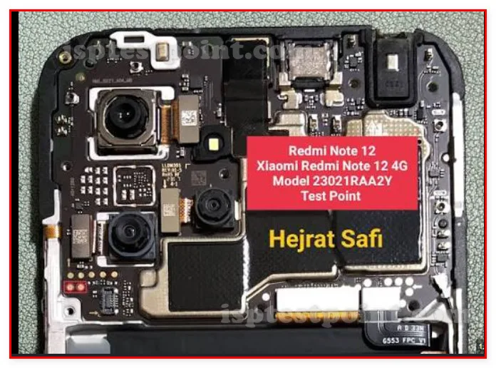
The Xiaomi Redmi Note 11 is a mid-range Android device that utilizes MediaTek Helio G88 processor architecture. Test points on this device enable technicians to perform critical repair operations including firmware restoration, FRP (Factory Reset Protection) bypass, and recovery from boot failures. Understanding the location and function of these test pads is essential for professional service workflows.

When to Use Test Points
Test points are accessed in specific troubleshooting scenarios:
- Dead-boot conditions where the device fails to power on or reach bootloader
- FRP lock removal when legitimate access credentials are unavailable
- Firmware corruption requiring complete ROM flashing via ISP mode
- Hardware-level diagnostics for eMMC communication verification
- NAND/eMMC read-write operations for data recovery workflows
These operations bypass normal software pathways and require direct hardware communication.
Accessing Test Points
Test points on the Redmi Note 11 are accessed through the device's main logic board. Begin by powering off the device completely and disconnecting any external power sources. Locate the motherboard test pads on the device's service side, typically positioned near the eMMC storage chip. Use a magnifying glass or digital microscope to identify precise pad locations. Establish continuity testing connections using fine-tipped test probes or ISP clip adapters. Connect your service tool (UMT, EasyJTAG, or equivalent) to the appropriate pins on your development computer. Verify all connections before initiating any read or write operations.
Common Test Point Locations
The primary test point cluster on Redmi Note 11 devices centers around the eMMC package. Key pads include CLK (clock signal), CMD (command line), and DAT0-DAT3 (data lines) which facilitate high-speed communication with storage. VCC and GND (power and ground) provide necessary voltage references. RST (reset) and VCCQ (I/O voltage) pins complete the essential ISP configuration. These pads are typically 0.5–1mm in size and located within 10mm of the main storage chip. When performing ISP operations, maintain steady pressure on all contact points to ensure reliable data transfer. Monitor voltage levels throughout the procedure to prevent component damage.
Safety Precautions
Technicians must observe strict safety protocols when working with test points. Always discharge static electricity before touching circuit boards using proper ESD wrist straps. Verify tool calibration and probe continuity before each session. Never apply voltage exceeding device specifications (typically 3.3V for logic lines). Avoid simultaneous connection of multiple test interfaces to prevent short-circuit conditions. Ensure proper ventilation and power supply isolation during ISP operations. If unexpected device heating occurs, immediately disconnect all tools and allow cool-down. Always document your procedure and maintain backup firmware images before attempting modifications. Improper test point contact can cause permanent hardware failure.
Pin / Test Point Reference
| Pin | Description |
|---|---|
| CLK | eMMC clock signal pad — Provides timing synchronization for data transfer |
| CMD | eMMC command/response line — Bidirectional communication with storage controller |
| DAT0 | eMMC data line 0 — Primary data signal path |
| DAT1 | eMMC data line 1 — Secondary data path |
| DAT2 | eMMC data line 2 — Tertiary data path |
| DAT3 | eMMC data line 3 — Quaternary data path |
| VCC | Primary power supply (3.3V) — Core voltage for eMMC operation |
| VCCQ | I/O voltage supply (1.8V/3.3V) — Logic level voltage reference |
| GND | Ground reference pad — Return path for all signals |
| RST | eMMC reset signal — Pulse low to reset storage controller |
Tools required: UMT (Universal Multi-Tool), EasyJTAG Plus, ISP eMMC Clip Adapter, Fine-tipped multimeter probes, Magnifying glass or digital microscope, ESD wrist strap, Soldering iron (micro-tip, 25W max)
Supported operations: Read Firmware (Full ROM backup), Write Firmware (ROM flashing), FRP Erase (Factory Reset Protection bypass), Dead-Boot Repair, eMMC Verification & Testing, NAND Data Recovery
⚠ Safety note: Operate at 3.3V logic levels only. Maintain ESD protection. Verify all connections before powering. Device will heat during prolonged ISP operations—monitor temperature. Incorrect pad contact risks permanent eMMC failure. Never apply voltage while probes are disconnected.

Comments (0)
Be the first to comment.