What Is ISP Pinout
ISP — In-System Programming — is a direct hardware method that allows technicians to communicate with a device's eMMC or UFS storage chip without relying on the host CPU or operating system. By soldering or probing specific pads on the motherboard, a programmer tool can read, write, or erase data at the memory level. This bypasses bootloader locks, Android security, and FRP (Factory Reset Protection) entirely, making it an essential technique when software-based methods fail.
For the Samsung Galaxy A90 5G (SM-A908), ISP access is particularly valuable because Qualcomm-based Samsung devices can be difficult to recover through standard ODIN flashing when the device is in a hard-bricked or boot-loop state. ISP provides a last-resort path to full firmware restoration or user data wipe.
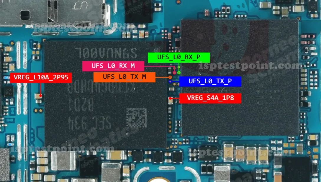
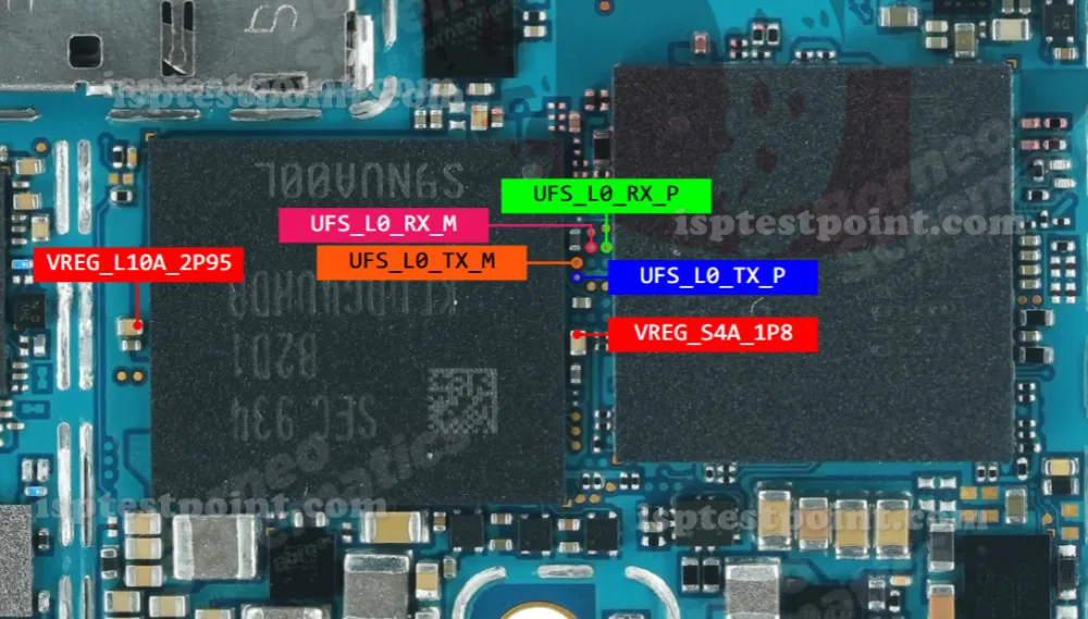
SM-A908 ISP Pinout Diagram
The SM-A908 uses a UFS 2.1 storage interface. The key ISP test points are located on the rear side of the main motherboard, near the UFS memory package. Because UFS uses a differential serial bus rather than the parallel eMMC bus, the pin names differ from classic eMMC ISP setups.
- VCC (2.9V) — Main supply voltage to UFS storage
- VCCQ (1.2V) — I/O supply for UFS interface logic
- GND — Common ground reference pad
- TX+/TX− — Differential transmit data lines (host to UFS)
- RX+/RX− — Differential receive data lines (UFS to host)
- REF_CLK — Reference clock input to UFS device
- RESET_N — Active-low hardware reset line
Note: Exact pad coordinates and silk-screen labels on the SM-A908 PCB are not publicly confirmed in widely verified schematics. Technicians should cross-reference with a verified board diagram or ISP box pinout card before probing.
When Technicians Use ISP
ISP access on the SM-A908 is most commonly used in the following scenarios:
- Dead Boot / Hard Brick: When the device shows no sign of life and ODIN cannot detect it, ISP allows direct firmware writing to storage.
- FRP Lock Removal: Google account locks that survive factory reset can be erased by wiping the relevant partition directly.
- Pattern/PIN Lock Bypass: User security locks stored in the userdata or metadata partition can be removed without full data wipe in some workflows.
- IMEI Repair: EFS partition backup and restore to recover corrupted or blank IMEI values.
- Full Firmware Backup: Cloning the complete UFS image for repair logging or restoration purposes.
Accessing the ISP Test Points
To reach the SM-A908 motherboard ISP pads, follow this general procedure:
- Power off the device completely and disconnect the battery as the first step.
- Remove the back glass using a heat gun set to approximately 80°C and plastic pry tools.
- Disconnect all flex cables and ribbon connectors before lifting the motherboard.
- Identify the UFS memory package on the board and locate adjacent test pads using a verified reference diagram.
- Use fine 30 AWG wire or ISP probe clips to connect to pads — avoid soldering directly on UFS balls unless reballing is intended.
- Connect to your ISP programmer, power the board externally at correct voltages, and initiate the operation.
Safety Tips and Precautions
Working at the ISP level carries significant risk. Observe the following precautions at all times:
- ESD Protection: Always wear an anti-static wrist strap and work on a grounded mat. UFS chips are highly sensitive to electrostatic discharge.
- Voltage Accuracy: Applying incorrect voltage — even briefly — to VCCQ or VCC lines can permanently destroy the UFS chip and render all data unrecoverable.
- No Battery Connected: Never perform ISP operations with the battery connected. Use a regulated bench power supply.
- Verified Pinout Only: Never guess pad locations. An incorrect connection to an adjacent power rail or RF line can cause board-level shorts.
- Irreversibility: Partition erase operations (FRP, userdata) cannot be undone. Confirm the operation before executing.
Pin / Test Point Reference
| Pin | Description |
|---|---|
| VCC | Main power supply to UFS storage, approximately 2.9V — Verify exact pad location on board |
| VCCQ | I/O logic supply for UFS interface, approximately 1.2V — Do not exceed rated voltage |
| GND | Ground reference pad for ISP programmer common ground |
| TX+ | Positive differential transmit line, host to UFS device — UFS differential pair — handle as matched pair |
| TX− | Negative differential transmit line, host to UFS device |
| RX+ | Positive differential receive line, UFS to host |
| RX− | Negative differential receive line, UFS to host |
| REF_CLK | Reference clock input line to UFS memory controller |
| RESET_N | Active-low reset signal for UFS device — Pull low to reset UFS before programming session |
Tools required: EasyJTAG Plus with UFS adapter, UFI Box, Medusa Pro II, RIFF Box 2 (UFS module), Regulated bench power supply (1.2V / 2.9V), Fine 30 AWG wire or ISP probe clips, Anti-static wrist strap and mat, Heat gun (for back glass removal), Plastic pry tools
Supported operations: Read Full UFS Firmware Dump, Write / Restore Firmware, FRP Erase, Pattern / PIN Lock Remove, EFS Backup and Restore (IMEI Repair), Dead Boot Repair, Userdata Partition Wipe
⚠ Safety note: Incorrect voltage on VCCQ or VCC will permanently destroy the UFS chip. Never connect battery during ISP. Use ESD protection at all times. Verify pad locations against a confirmed schematic before probing.

Comments (0)
Be the first to comment.