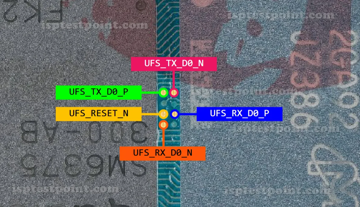
What Is ISP Pinout
ISP (In-System Programming) is a direct hardware method that allows technicians to communicate with a device's eMMC or UFS storage chip without relying on the device's main CPU boot process. By connecting a compatible flasher tool directly to the storage interface test points on the PCB, the technician can read, write, or erase firmware at the chip level. This approach bypasses software locks, corrupted bootloaders, and even a completely unresponsive device, making it the preferred recovery path when standard USB-based flashing fails. For the Samsung SM-A236 5G, ISP access targets the UFS interface pads exposed on the motherboard, enabling full firmware restoration, FRP account removal, and partition-level operations.
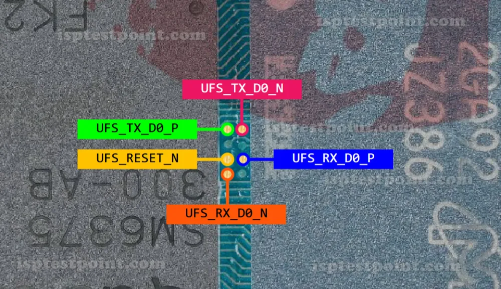
SM-A236 ISP Test Point Map
The Samsung SM-A236 5G uses a UFS 2.1 storage interface. The ISP test points are located on the back side of the main PCB, near the UFS storage chip. Because this is a second-revision (V2) board layout, pad positions may differ slightly from the original A236 V1. The key signal pads to identify are listed below:
- CLK – UFS reference clock line
- DATA0 (DIN+/DIN−) – Differential data pair for UFS lane 0
- VCC – Main storage power supply (typically 2.9 V)
- VCCQ – I/O voltage rail for UFS (typically 1.8 V)
- GND – Common ground reference pad
- RST – UFS reset signal line
Exact pad coordinates and silkscreen labels are board-revision-specific and should be verified against a current SM-A236 V2 PCB diagram before probing.
When Technicians Use ISP
ISP access on the SM-A236 5G is typically required in three scenarios. First, dead-boot repair: if the device shows no sign of life after a failed OTA update, interrupted flash, or bootloader corruption, ISP allows the technician to rewrite firmware directly to storage. Second, pattern or FRP lock removal: when EDL (Emergency Download Mode) is inaccessible due to security fuses or a non-functional power button, ISP provides an alternative path to erase the FRP partition. Third, as a chip-off alternative: rather than physically removing the UFS chip — a destructive and high-risk procedure — ISP preserves the chip in place while still allowing full read and write access.
How to Access ISP Points
Follow this procedure carefully:
- Power off the device completely and disconnect the battery connector on the PCB.
- Disassemble the device to expose the main motherboard.
- Identify the UFS ISP test pads using a verified SM-A236 V2 board schematic.
- Solder thin 30 AWG jumper wires to the CLK, DATA, VCC, VCCQ, GND, and RST pads.
- Connect the jumper wires to the appropriate ISP socket or cable on your flasher box (e.g., EasyJTAG Plus or UMT ISP adapter).
- Launch the flasher software, select the SM-A236 or matching UFS profile, and power the board through the tool — do not reconnect the battery.
- Execute the desired operation (read, write, or FRP erase) and wait for completion before disconnecting.
Safety Tips and Precautions
Always verify supply voltages before applying power: VCC must not exceed 3.0 V and VCCQ must not exceed 1.95 V or UFS damage will occur. Use ESD-safe mats, wrist straps, and antistatic tools throughout the procedure. Never work on a PCB with the battery connected during soldering. Back up the full UFS dump before writing any new firmware — restoring from a bad image without a backup can result in permanent data loss. If you are not confident in pad identification, cross-reference at least two independent SM-A236 V2 schematics before making contact. Avoid excessive heat on pads smaller than 0.3 mm to prevent pad lift.
Pin / Test Point Reference
| Pin | Description |
|---|---|
| CLK | UFS reference clock signal pad on PCB — Exact pad location requires SM-A236 V2 schematic verification |
| DAT0+/DAT0- | UFS differential data lane 0 pair (positive and negative) — UFS uses differential signaling; handle as a pair |
| VCC | Main UFS storage supply voltage — typically 2.9 V — Do not exceed 3.0 V |
| VCCQ | UFS I/O voltage rail — typically 1.8 V — Do not exceed 1.95 V |
| GND | Common ground reference pad — Multiple ground pads may be present; use nearest to UFS chip |
| RST | UFS reset signal line — Required by some ISP tools for proper UFS initialization |
Tools required: EasyJTAG Plus with UFS ISP adapter, UMT (Ultimate Multi Tool) with ISP cable, Medusa Pro II, 30 AWG soldering wire, Hot air rework station, ESD mat and wrist strap, Verified SM-A236 V2 PCB schematic
Supported operations: Dead Boot Repair, Full UFS Dump (Read Firmware), Write Firmware, FRP Erase, IMEI Repair (where legally permitted), Partition-level Operations
⚠ Safety note: VCC max 3.0 V, VCCQ max 1.95 V. Always disconnect battery before soldering. Use ESD protection. Back up full UFS dump before any write operation.

Comments (0)
Be the first to comment.