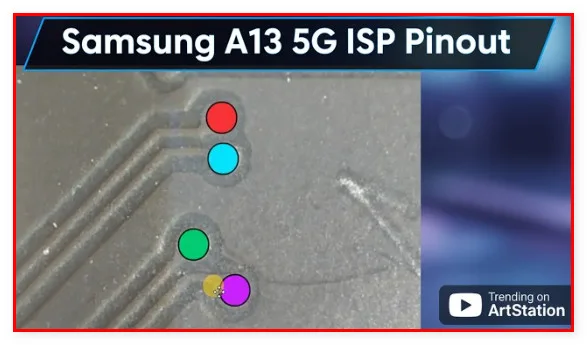
What Is ISP Pinout
ISP (In-System Programming) is a direct hardware interface method that allows technicians to communicate with a device's flash storage — eMMC or UFS — by probing dedicated test pads on the PCB rather than relying on the device's bootloader or USB port. When a Samsung A13 5G refuses to boot, is locked in a bootloop, or has a corrupted partition table, standard USB-based flashing tools simply cannot establish a connection. ISP bypasses the processor's boot sequence entirely, giving the programmer hardware-level read and write access to the storage chip. This makes it an essential technique for dead boot recovery, FRP credential removal, IMEI repair preparation, and full firmware restoration on devices that are otherwise unresponsive.

SM-A136U1 ISP Pin Locations
The Samsung SM-A136U1 uses a UFS 2.1 flash storage architecture. The ISP test points are located on the back side of the main PCB, in the lower-central region near the UFS package. Because the A136U1 is a carrier-specific US variant, minor PCB revisions between production batches may shift pad positions slightly. The standard UFS ISP signals to locate are listed below. Exact silk-screen labels or coordinate measurements are not universally confirmed across all board revisions and are marked uncertain.
- CLK — UFS reference clock signal
- DATA0 (DIN/DOUT) — Primary bidirectional data line
- VCC — Flash core supply (typically 2.9 V–3.0 V)
- VCCQ — I/O supply voltage (typically 1.8 V)
- GND — Common ground reference
- RST — Reset line (present on some board variants)
Use a high-resolution PCB diagram or your ISP programmer's auto-detect feature alongside a confirmed board photo before soldering any wires.
When Technicians Use ISP
ISP is the preferred repair path when the device displays no signs of life, when Download Mode is inaccessible, when the bootloader is damaged, or when the eMMC/UFS partition is so corrupt that Odin and similar tools time out. It is also used when software FRP removal methods have been exhausted and a direct storage wipe is required. ISP is not a first-resort tool — it is reserved for cases where every software-side approach has already failed.
Accessing the Test Points
Begin by fully disassembling the device and removing the PCB. Clean the target test pad area with IPA and a soft brush. Under magnification, tin each test pad lightly before attaching 30 AWG or finer enameled wire. Route wires carefully to avoid bridging adjacent pads. Connect the wires to your ISP programmer's corresponding header pins, power on the programmer first, then apply board power via the VCC and VCCQ lines. Launch your software, select the MT6833 or UFS 2.1 target profile, and initiate detection before proceeding with any read or write operation.
Safety Tips and Precautions
Never exceed 1.8 V on the VCCQ line or 3.0 V on the VCC line — overvoltage will permanently destroy the UFS die. Always discharge any residual board capacitance before probing. Use a regulated bench power supply with current limiting set to 500 mA or less. Confirm polarity on every wire before powering up. Keep the work area ESD-safe, and never attempt ISP on a board still attached to the battery connector. Back up any readable data before performing erase or write operations, as they are irreversible.
Pin / Test Point Reference
| Pin | Description |
|---|---|
| CLK | UFS clock signal test pad — Exact pad coordinates unconfirmed; verify against board photo |
| DAT0 | Primary UFS bidirectional data line — May be labeled DIN/DOUT depending on programmer |
| VCC | UFS core power supply — typically 2.9 V to 3.0 V |
| VCCQ | UFS I/O voltage — typically 1.8 V — Do not exceed 1.8 V |
| GND | Ground reference point on PCB — Multiple ground pads available near UFS package |
| RST | Reset line — present on select board revisions — Confirm presence on your specific PCB revision before use |
Tools required: EasyJTAG Plus, UFI Box, Medusa Pro II, UMT Pro (UFS module), Riff Box 2, 30 AWG enameled copper wire, Regulated bench power supply, Digital multimeter, Stereo microscope or magnification loupe
Supported operations: Read Firmware / Full Dump, Write Firmware / Flash Restore, FRP Erase, Dead Boot Repair, Partition Table Repair, IMEI Area Backup
⚠ Safety note: Do not exceed 3.0 V VCC or 1.8 V VCCQ. Use current-limited PSU ≤500 mA. ESD precautions mandatory. Verify all pin assignments against a confirmed PCB photo before powering.

Comments (0)
Be the first to comment.