What Is ISP Pinout
ISP (In-System Programming) is a chip-level repair technique that allows technicians to communicate directly with a device's eMMC or UFS storage by accessing dedicated test pads on the motherboard. Rather than relying on the device's operating system, bootloader, or USB port, ISP bypasses all software layers and connects specialized hardware directly to the storage chip's data lines. This method is essential when a phone is completely unresponsive, stuck in a bootloop, or has suffered a corrupt firmware flash that prevents normal USB-based recovery. For the Samsung SM-A136U, ISP access enables operations such as full firmware re-flash, FRP (Factory Reset Protection) bypass, and IMEI repair at the hardware level.

SM-A136U ISP Pinout Map
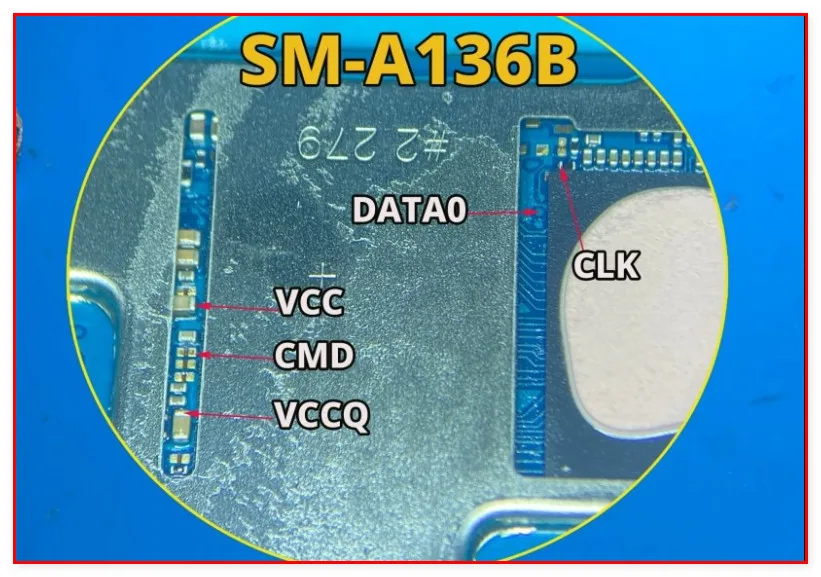
The Samsung SM-A136U uses a UFS 2.1 storage interface. The ISP test pads are located on the rear side of the motherboard, typically near the UFS storage IC. The primary pads required for ISP connection are as follows:
- CLK – Clock signal line; synchronizes data transfer between the tool and UFS chip.
- CMD – Command line; carries read/write instructions from the programming tool.
- DAT0 – Primary data line for UFS communication.
- VCC – Main power supply to the storage chip (typically 2.9V–3.0V).
- VCCQ – I/O voltage supply line (typically 1.8V for UFS).
- GND – Ground reference pad; must be connected for stable signal integrity.
Exact pad coordinates and silkscreen labels on the SM-A136U PCB vary by board revision. Technicians should cross-reference physical board markings with a verified pinout diagram from a trusted ISP tool vendor before soldering or probing.
When Technicians Use ISP
ISP is the go-to method when standard repair paths have failed. Common scenarios include: a device that powers on but immediately powers off (dead boot), a phone stuck in a Samsung logo bootloop after a failed OTA or manual flash, an FRP lock that cannot be cleared through ADB or download mode, and situations where the USB charging port is physically damaged and USB-based flashing is impossible. ISP restores access to the storage directly, making it the last reliable option before board-level component replacement.
Accessing the Test Points
Follow these steps to safely connect to the SM-A136U ISP pads:
- Fully disassemble the device and remove the motherboard, disconnecting the battery first.
- Clean the target pad area with isopropyl alcohol (99%) and a soft brush.
- Under magnification, identify the CLK, CMD, DAT0, VCC, VCCQ, and GND pads using a verified diagram.
- Solder fine gauge (30–32 AWG) wire to each pad, or use a compatible ISP pogo-pin adapter if available.
- Connect wires to your ISP tool's corresponding interface header in the correct order.
- Power the board through the tool's regulated supply — do not connect the battery during the ISP session.
- Launch your ISP software, select the MediaTek UFS platform, and initiate detection before proceeding with any read or write operation.
Safety Tips and Precautions
Working at the ISP level carries significant risk of permanent board damage if proper precautions are not followed. Always verify voltage output from your tool before connecting — VCCQ must not exceed 1.8V and VCC must not exceed 3.0V on this platform. Use a current-limited bench power supply where possible. Never apply excessive heat when soldering to test pads; small pads lift easily and cannot be repaired without advanced rework skills. Ensure your ISP tool firmware is up to date and explicitly supports the MT6833 UFS platform. Do not connect the battery while the ISP tool is powering the board, as voltage conflicts can destroy the storage IC or CPU. Always perform a full backup (read) before any write or erase operation.
Pin / Test Point Reference
| Pin | Description |
|---|---|
| CLK | Clock signal pad for UFS communication timing — Exact pad location varies by PCB revision; verify with board diagram |
| CMD | Command line carrying read/write instructions to the UFS chip |
| DAT0 | Primary data line for UFS storage interface |
| VCC | Main power supply to UFS storage IC, typically 2.9V–3.0V — Do not exceed rated voltage |
| VCCQ | I/O voltage supply for UFS interface, typically 1.8V — Critical: overvoltage will destroy UFS chip |
| GND | Ground reference pad required for stable ISP connection |
Tools required: EasyJTAG Plus, UMT (Ultimate Multi Tool), Medusa Pro II, UFi Box, RIFF Box 2, BST Dongle
Supported operations: Read Firmware, Write Firmware, FRP Erase, Dead Boot Repair, IMEI Repair, Full eMMC/UFS Backup
⚠ Safety note: VCCQ must not exceed 1.8V; VCC must not exceed 3.0V. Disconnect battery before connecting ISP tool. Overvoltage or reverse polarity will permanently destroy the UFS chip and CPU.

Comments (0)
Be the first to comment.