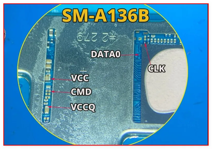
What Is ISP Pinout
ISP (In-System Programming) pinout is a hardware-level technique that allows repair technicians to communicate directly with the eMMC or UFS storage chip on the Samsung SM-A136B motherboard, bypassing the device's main processor and software stack entirely. Instead of relying on Android's bootloader or Samsung's Odin flash protocol, the ISP method accesses the storage through dedicated test pads exposed on the PCB. For the SM-A136B, which runs on the MediaTek Dimensity 700 platform, ISP gives technicians a last-resort path to read, write, or erase firmware and user data when no other software method is viable. This is especially relevant because MediaTek ISP differs slightly from Qualcomm EDL routines, making direct pad access one of the most reliable fallback options available.

When Technicians Use ISP
ISP access on the Samsung SM-A136B becomes necessary in several critical repair scenarios:
- Dead Boot: The device powers on but does not progress past a black screen, often caused by a failed OTA update or interrupted flash attempt.
- FRP Lock Removal: When Factory Reset Protection cannot be bypassed through standard software tools or ADB methods, ISP allows direct erasure of the FRP partition.
- Locked Bootloader with No EDL: MediaTek devices do not use Qualcomm's EDL mode; ISP becomes the primary hardware bypass route.
- IMEI or EFS Restoration: Reading and restoring a corrupted EFS partition requires direct eMMC/UFS access.
- Firmware Corruption: If the system partition is damaged beyond software repair, ISP allows a full firmware write.
SM-A136B ISP Test Points
The ISP test points on the Samsung SM-A136B are located on the rear side of the motherboard, near the UFS storage chip. Technicians must remove the rear cover, battery, and motherboard shielding to access them. The key signals required are:
- CMD: Command line between host and UFS controller
- CLK: Clock signal pad for synchronization
- DAT0: Primary data line for read/write operations
- VCC: Main power supply to the storage (typically 2.9V–3.0V)
- VCCQ: I/O power rail (typically 1.8V)
- GND: Ground reference pad
Exact pad coordinates on the PCB are not publicly confirmed in standardized documentation and should be verified using a board-level schematic or a trusted ISP pad diagram before probing.
ISP Access Procedure
Follow these steps to perform ISP access on the SM-A136B:
- Power off the device completely and discharge any residual voltage.
- Disassemble the device and remove the motherboard from the chassis.
- Locate and clean the ISP test pads using isopropyl alcohol (99%).
- Solder thin wire leads or use a dedicated ISP probe clip to connect to CMD, CLK, DAT0, VCC, VCCQ, and GND.
- Connect the wiring harness to your ISP tool (e.g., EasyJTAG Plus or UMT).
- Launch the appropriate software, select MediaTek UFS protocol, and detect the chip.
- Perform the desired operation: full read, firmware write, or partition erase.
- After completion, remove probes carefully and reassemble the device.
Safety Tips and Precautions
Working at the ISP level carries significant risk of permanent damage if precautions are not followed:
- Never exceed 3.0V on the VCC rail or 1.8V on the VCCQ rail — overvoltage will destroy the UFS chip instantly.
- Always verify pad identity with a multimeter in continuity mode before applying power.
- Avoid applying solder bridges between adjacent pads; the pitch is extremely fine on modern Samsung boards.
- Use a regulated bench power supply rather than the device's own battery during ISP operations.
- Static discharge can kill the UFS chip — always use an ESD wrist strap and mat.
- Back up a full eMMC read before writing any firmware to preserve the original state.
Pin / Test Point Reference
| Pin | Description |
|---|---|
| CMD | Command signal line between ISP tool and UFS controller — Exact pad location unconfirmed; verify with schematic |
| CLK | Clock signal pad used for synchronizing data transfer — Exact pad location unconfirmed; verify with schematic |
| DAT0 | Primary data line for read/write operations to UFS storage — Exact pad location unconfirmed; verify with schematic |
| VCC | Main power supply to UFS storage chip, typically 2.9V–3.0V — Do not exceed 3.0V |
| VCCQ | I/O voltage rail for UFS interface signaling, typically 1.8V — Do not exceed 1.8V |
| GND | Ground reference pad, required for all ISP connections — Multiple GND pads available on board; any confirmed ground point is acceptable |
Tools required: EasyJTAG Plus, UMT (Ultimate Multi Tool), Medusa Pro II, UFI Box, ISP probe wires or clip adapter, Regulated bench power supply, Multimeter, Soldering station (fine tip), ESD wrist strap and mat
Supported operations: Full eMMC/UFS Read, Firmware Write, FRP Erase, Dead Boot Repair, IMEI / EFS Restoration, Partition Backup and Restore, Pattern/PIN Lock Removal
⚠ Safety note: UFS VCC max 3.0V, VCCQ max 1.8V. Overvoltage permanently destroys storage. Always ESD-protect and verify pad identity before powering. Full read backup strongly recommended before any write operation.

Comments (0)
Be the first to comment.