What Is ISP Pinout
ISP (In-System Programming) is a method that allows technicians to communicate directly with the eMMC flash storage chip on a device's motherboard, bypassing the main CPU and operating system entirely. On the Samsung SM-A12 (model A125), which runs on the MediaTek Helio P35 platform, the ISP interface exposes the raw eMMC bus signals through dedicated test pads on the PCB. By connecting a compatible programmer tool to these pads, a technician can read, write, or erase the NAND flash at the hardware level. This makes ISP an indispensable method when software-based approaches are no longer viable.

When Technicians Use ISP
ISP is typically chosen when conventional repair paths have failed or are unavailable. Common scenarios where ISP is the preferred approach on the SM-A12 include:
- Dead Boot Repair: When the device will not power on and USB is unresponsive, ISP provides a direct path to reflash the bootloader or full firmware image.
- FRP (Factory Reset Protection) Unlock: When a device is locked to a Google account and normal unlock procedures are blocked, ISP allows direct erasure of the FRP partition.
- Broken USB Port: Physical damage to the USB/charging connector makes PC-based flashing impossible; ISP bypasses the port entirely.
- Corrupted Bootloader: Partial or failed OTA updates that brick the device can be recovered by rewriting critical partitions through the ISP interface.
SM-A12 ISP Test Points
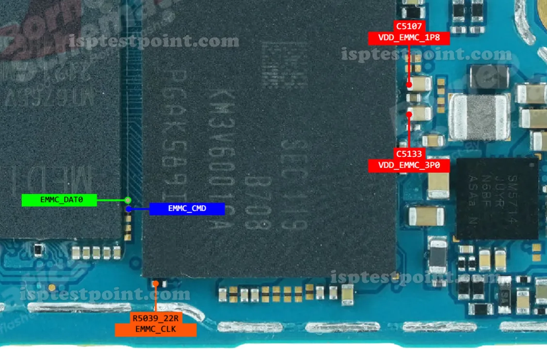
The following test point assignments apply to the Samsung SM-A12 (A125) PCB. These pads are located on the back side of the main board, near the eMMC chip area. Use a precision multimeter to confirm continuity before connecting any programmer.
- CLK – eMMC clock signal test pad
- CMD – Command line test pad
- DAT0 – Data line 0 (minimum required for basic ISP operations)
- DAT1–DAT7 – Extended data lines for full 8-bit eMMC bus width
- GND – Ground reference pad (multiple available near the eMMC footprint)
- VCC – 3.3V eMMC power supply pad
- VCCQ – 1.8V I/O voltage pad
Note: Exact pad coordinates and silkscreen labels are not confirmed in public documentation for this model. Use a board schematic or verified repair map before soldering.
Connecting the ISP Interface
Follow these steps when attaching a programmer to the SM-A12 ISP test points:
- Disconnect the battery completely before making any connections.
- Clean the target test pads with isopropyl alcohol and a soft brush.
- Solder fine gauge (0.1mm) enamelled wire to each test pad or use spring-loaded ISP clips.
- Connect wires to the corresponding ISP socket on your programmer (EasyJTAG Plus or UMT box).
- Set programmer voltage to 1.8V VCCQ / 3.3V VCC before powering the session.
- Launch the software, select eMMC ISP mode, and identify the chip before proceeding with any read or write operation.
Safety Tips Before You Start
Taking proper precautions protects both the device and the technician:
- Power Off: Always confirm the battery is fully disconnected. Residual charge can damage test pads or the programmer.
- ESD Protection: Wear an anti-static wrist strap and work on an ESD mat at all times.
- Voltage Check: Verify your programmer outputs the correct voltages (1.8V VCCQ, 3.3V VCC) before connecting to the board.
- Backup First: Always perform a full eMMC read/dump before attempting any write or erase operation.
- Flux and Heat: Use minimal flux and low-temperature solder (138°C bismuth alloy recommended) to avoid lifting pads.
Pin / Test Point Reference
| Pin | Description |
|---|---|
| CLK | eMMC clock signal — Exact pad location unconfirmed; verify with board schematic |
| CMD | eMMC command line — Exact pad location unconfirmed |
| DAT0 | eMMC data line 0 — minimum required for ISP — Exact pad location unconfirmed |
| DAT1 | eMMC data line 1 — Exact pad location unconfirmed |
| DAT2 | eMMC data line 2 — Exact pad location unconfirmed |
| DAT3 | eMMC data line 3 — Exact pad location unconfirmed |
| DAT4 | eMMC data line 4 — Exact pad location unconfirmed |
| DAT5 | eMMC data line 5 — Exact pad location unconfirmed |
| DAT6 | eMMC data line 6 — Exact pad location unconfirmed |
| DAT7 | eMMC data line 7 — Exact pad location unconfirmed |
| VCC | eMMC core power supply — 3.3V — Exact pad location unconfirmed |
| VCCQ | eMMC I/O voltage — 1.8V — Exact pad location unconfirmed |
| GND | Ground reference — multiple points available near eMMC chip |
Tools required: EasyJTAG Plus, UMT (Ultimate Multi Tool), Medusa Pro II, RIFF Box 2, Fine gauge enamelled wire (0.1mm), Precision soldering iron (low-temperature tip), Digital multimeter, Anti-static wrist strap and ESD mat
Supported operations: Read Firmware (eMMC Dump), Write Firmware, FRP Erase, Dead Boot Repair, Bootloader Repair, IMEI Repair (subject to local law), Pattern/PIN Unlock
⚠ Safety note: Always disconnect the battery before connecting ISP wires. Set programmer to 1.8V VCCQ and 3.3V VCC. Incorrect voltage will permanently damage the eMMC. Always create a full backup before any write operation.

Comments (0)
Be the first to comment.