What Is ISP Pinout
ISP (In-System Programming) is a hardware-level data access method that allows technicians to communicate directly with a device's NAND flash memory (eMMC) without using the normal USB boot process. By identifying and soldering fine-wire connections to specific test pads on the PCB, a compatible box or adapter can read, write, or erase the eMMC chip directly. This approach bypasses the CPU's software stack entirely, making it invaluable when a device cannot boot, the USB port is damaged, or standard software unlock methods have failed. For the Samsung SM-A10S (A107), ISP access targets the eMMC interface lines exposed as test points on the motherboard.

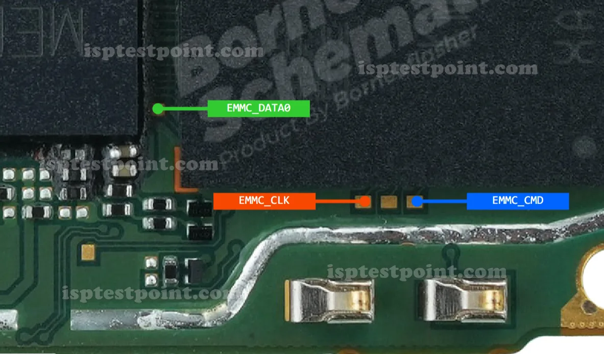
SM-A10S ISP Pinout Diagram
The following test points are used to establish an ISP connection on the A107 board. These pads are located on the back side of the motherboard, typically clustered near the eMMC chip. Wire gauge of 30–36 AWG is recommended for reliable contact.
- CLK — eMMC clock signal
- CMD — Command line for eMMC communication
- DAT0 — Primary data line (minimum required for 1-bit mode)
- VCC — eMMC core power supply (typically 3.3 V)
- VCCQ — eMMC I/O power supply (typically 1.8 V)
- GND — Common ground reference
Exact pad coordinates on the A107 PCB can vary between board revisions and regional manufacturing batches. Always verify pad identity using a board-level schematic or a verified photo reference before soldering.
When Technicians Use ISP
ISP access on the SM-A10S is typically required in the following scenarios:
- FRP (Factory Reset Protection) bypass — when the device is locked to a Google account after a factory reset and conventional ADB/download mode methods are blocked.
- Dead boot repair — when the device fails to power on due to a corrupt bootloader or failed OTA update.
- User data recovery — reading a raw eMMC dump from a device with a cracked screen or non-functional USB controller.
- Firmware flashing — writing a clean firmware image directly to eMMC when Download Mode is inaccessible.
How to Access the Test Points
Follow these steps carefully to establish an ISP connection on the A107:
- Power off the device completely and remove the back cover and battery.
- Detach the motherboard from the chassis following standard Samsung disassembly procedure.
- Identify the ISP test pads using a verified board diagram for the A107.
- Carefully solder 30–36 AWG enameled wires to CLK, CMD, DAT0, VCC, VCCQ, and GND pads.
- Connect the wires to your ISP adapter or compatible box socket in the correct pin order.
- Launch your ISP software, select the correct eMMC type, and initiate the desired operation.
- After completion, desolder the wires, clean the pads with IPA, and reassemble the device.
Safety Tips and Precautions
ISP work carries real risk of permanent board damage if performed incorrectly. Observe the following precautions:
- Never apply more than 3.3 V to VCC or 1.8 V to VCCQ — overvoltage will destroy the eMMC.
- Confirm pad identity with a multimeter in continuity mode before applying power.
- Use a regulated bench power supply rather than relying solely on the ISP box voltage rail.
- Avoid excessive heat when soldering to small test pads; use flux and a fine-tip iron below 320 °C.
- Always back up a full eMMC dump before erasing or writing any partition.
- Work in an ESD-safe environment with a grounded wrist strap.
Pin / Test Point Reference
| Pin | Description |
|---|---|
| CLK | eMMC clock signal test pad — Exact pad location varies by board revision; verify before soldering |
| CMD | eMMC command line test pad |
| DAT0 | Primary eMMC data line; minimum required for 1-bit ISP mode |
| VCC | eMMC core power supply — typically 3.3 V |
| VCCQ | eMMC I/O power supply — typically 1.8 V |
| GND | Ground reference pad |
Tools required: EasyJTAG Plus, UMT (Ultimate Multi Tool) with ISP adapter, Medusa Pro II, RIFF Box 2, 30–36 AWG enameled wire, Fine-tip soldering iron (< 320 °C), Flux, Regulated bench power supply, Multimeter
Supported operations: FRP Erase, Dead Boot Repair, Read Firmware / eMMC Dump, Write Firmware, User Lock / PIN / Pattern Remove
⚠ Safety note: Do not exceed 3.3 V on VCC or 1.8 V on VCCQ. Confirm all pad identities before powering. ESD precautions mandatory. Full dump backup required before any write operation.

Comments (0)
Be the first to comment.