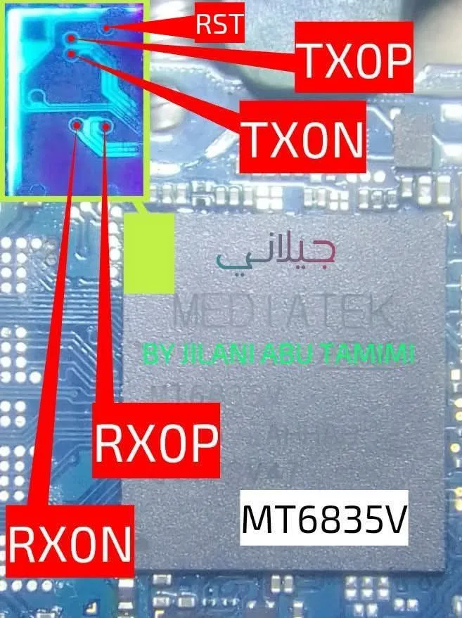
What Is ISP Pinout
ISP (In-System Programming) is a hardware-level method that allows technicians to communicate directly with the NAND flash memory chip on a device's PCB without relying on the phone's operating system, bootloader, or USB interface. On the Samsung SM-A066 (Galaxy A06 5G), ISP involves identifying specific test pads on the motherboard that correspond to the eMMC or UFS bus signals — CLK, CMD, DAT0 through DAT3, VCC, VCCQ, and GND. By connecting a compatible ISP programmer directly to these pads, a technician gains raw read/write access to the storage chip, bypassing all software-level security layers. This makes ISP an essential technique for data recovery, firmware restoration, and security bypass when conventional methods have failed.

When Technicians Use ISP
ISP is typically a last-resort or specialist method deployed under several critical conditions:
- Dead Boot: The device powers on but fails to boot due to corrupted firmware or a bad system partition write.
- FRP Lock: Factory Reset Protection is active and cannot be bypassed via ADB, Download Mode, or software tools.
- Failed EDL/Download Mode: The MediaTek BROM or Download Mode is inaccessible due to security fuse configurations or hardware damage.
- Pattern/PIN Lock: Screen lock credentials are unknown and the device cannot be reset through conventional recovery.
- IMEI Repair: The IMEI has been corrupted or erased and must be restored at the partition level.
In all these scenarios, ISP provides a direct hardware path that circumvents software restrictions entirely.
SM-A066 ISP Test Points
The SM-A066 is powered by the MediaTek MT6833 (Dimensity 700) SoC. The eMMC/UFS storage bus test points are located on the rear side of the main PCB. Due to the compact PCB layout typical of A-series budget devices, pads may be closely spaced and require fine-tip probing.
- CLK: Clock signal pad — exact coordinates unconfirmed, refer to verified PCB diagram
- CMD: Command line pad
- DAT0: Primary data line
- DAT1–DAT3: Additional data bus lines
- VCC: 2.9V storage power supply pad
- VCCQ: 1.8V I/O voltage pad
- GND: Common ground — available at multiple shield frame contact points
Exact pad coordinates for this model are not yet fully verified in public databases and are marked uncertain. Always cross-reference with a hardware-confirmed PCB map before proceeding.
Step-by-Step Access Procedure
Follow this process carefully when performing ISP on the SM-A066:
- Fully disassemble the device and isolate the main PCB from the chassis.
- Clean the PCB surface around the test point area using isopropyl alcohol (99%).
- Identify and confirm each ISP pad using a multimeter in continuity mode against a verified pinout diagram.
- Solder fine 30 AWG wire leads or use spring-pin ISP jig clips to each pad.
- Connect the wires to your ISP programmer (e.g., EasyJTAG Plus or UMT Pro ISP adapter).
- Power the board at the correct voltage (do NOT apply USB power simultaneously).
- Launch the programmer software, select the MT6833 or auto-detect the eMMC/UFS chip.
- Perform a full dump read before any write or erase operation.
Safety Warnings and Best Practices
ISP work on the SM-A066 carries real risk of permanent damage if proper precautions are not followed:
- ESD Protection: Always wear an anti-static wrist strap and work on a grounded mat.
- Voltage Limits: The storage bus operates at 1.8V I/O (VCCQ). Never exceed this — overvoltage will destroy the storage chip instantly.
- Full Backup First: Always perform a complete NAND dump before any erase or write operation. Store backups securely.
- No Concurrent Power: Do not connect USB and ISP power simultaneously — conflicting voltages can damage the SoC or PMIC.
- Double-Check Connections: A misidentified pad can short critical power rails. Verify every connection before powering on.
Pin / Test Point Reference
| Pin | Description |
|---|---|
| CLK | eMMC/UFS clock signal test pad on rear PCB — Exact location unverified — confirm with hardware PCB diagram |
| CMD | Command line for eMMC/UFS communication — Exact location unverified |
| DAT0 | Primary data line (D0) of storage bus — Exact location unverified |
| DAT1 | Data line 1 of storage bus — Exact location unverified |
| DAT2 | Data line 2 of storage bus — Exact location unverified |
| DAT3 | Data line 3 of storage bus — Exact location unverified |
| VCC | Storage chip power supply — typically 2.9V — Verify voltage before applying |
| VCCQ | I/O voltage rail for storage bus — 1.8V — Critical: do not exceed 1.8V |
| GND | Ground — available at PCB shield frame contact points — Multiple accessible points on board edge |
Tools required: EasyJTAG Plus, UMT Pro (ISP Mode), Medusa Pro II, RIFF Box 2, 30 AWG soldering wire or ISP spring-pin jig, Anti-static wrist strap, 99% isopropyl alcohol, Fine-tip soldering iron
Supported operations: Read Firmware, Write Firmware, FRP Erase, Dead Boot Repair, Pattern/PIN Lock Remove, IMEI Repair, Full NAND Dump, Partition-Level Erase
⚠ Safety note: VCCQ must not exceed 1.8V. Always dump full NAND before any write. Never apply USB and ISP power simultaneously. ESD protection mandatory.

Comments (0)
Be the first to comment.