What Is ISP Pinout
ISP (In-System Programming) pinout is a hardware-level technique that allows technicians to communicate directly with a device's NAND flash memory chip — bypassing the main CPU entirely. On the Samsung SM-A032 (Galaxy A03 Core), the eMMC flash storage is accessible via dedicated test pads on the motherboard. By connecting a compatible programmer tool to these pads, a technician can read, write, or erase data at the raw flash level. This method is especially valuable when the device's operating system is unresponsive, the bootloader is locked, or standard software-based solutions have failed. ISP access effectively treats the eMMC as an external storage device, granting full low-level control.

When Technicians Use ISP
ISP is not a first-resort tool — it is used when conventional methods are exhausted. Common scenarios where ISP becomes necessary on the SM-A032 include:
- Dead Boot / Brick Recovery: When the device fails to power on after a failed firmware flash or corrupted bootloader.
- FRP (Factory Reset Protection) Bypass: When a device is locked to a previous Google account and cannot be unlocked through software menus.
- Pattern or PIN Lock Removal: When the user has forgotten their screen lock credentials and ADB/download mode is inaccessible.
- IMEI Repair: In some cases, restoring a corrupted or null IMEI via direct flash write operations.
- Firmware Backup and Restore: Creating a full eMMC dump before performing risky repairs, or restoring a known-good dump afterward.
SM-A032 ISP Test Points
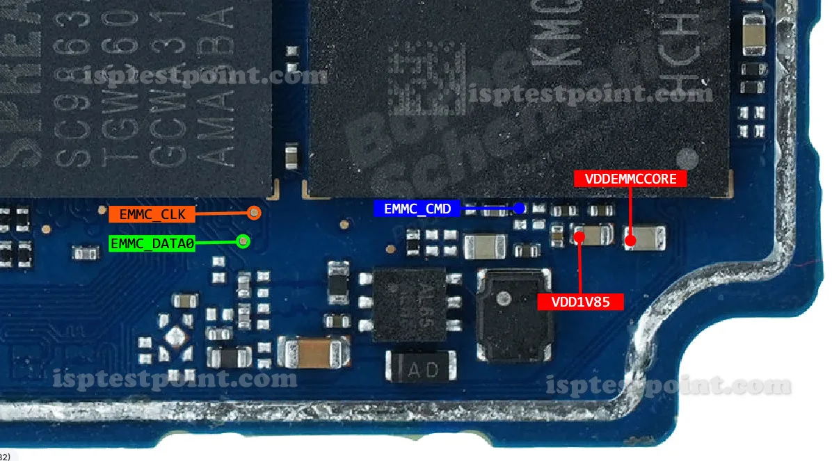
The following eMMC ISP test points are located on the SM-A032 motherboard. These pads are typically found near the eMMC chip on the rear side of the PCB. Use a magnifying tool or microscope to locate them precisely before soldering or probing.
- CLK — Clock signal line; synchronizes data transfer between programmer and eMMC.
- CMD — Command line; sends read/write instructions to the flash chip.
- DAT0 — Primary data line for eMMC communication.
- VCC — Main power supply to the eMMC (typically 3.3V).
- VCCQ — I/O voltage supply for signal lines (typically 1.8V).
- GND — Ground reference for the circuit.
Note: Exact pad coordinates on the SM-A032 PCB are not universally published. Refer to a board-level schematic or a verified test point diagram from your programmer tool's database before proceeding.
Step-by-Step Access Procedure
Follow this general procedure when connecting an ISP programmer to the SM-A032:
- Fully disassemble the device and remove the motherboard safely.
- Clean the PCB surface around the eMMC test pads using isopropyl alcohol.
- Using fine-tipped probes or soldered wire leads, connect CLK, CMD, DAT0, VCC, VCCQ, and GND to your programmer adapter.
- Launch your programmer software (e.g., EasyJTAG Plus or UMT), select eMMC ISP mode, and choose the SM-A032 or a compatible Unisoc SC9863A profile.
- Power the board via the VCC/GND lines from the programmer — do NOT insert the battery.
- Initiate detection, then proceed with your desired operation: dump, erase, or write.
Safety Tips and Precautions
ISP work carries significant risk if performed carelessly. Observe the following precautions:
- Voltage discipline: Always verify VCC (3.3V) and VCCQ (1.8V) levels before powering. Over-voltage will permanently damage the eMMC chip.
- No battery during ISP: Never insert the battery while the programmer is supplying power — this can cause shorts or board damage.
- Backup first: Always create a full eMMC dump before writing or erasing. This is your only recovery option if a write operation fails.
- Confirm pad identity: Misidentifying pads and applying power to the wrong point is the most common cause of board damage. Double-check with a multimeter in continuity mode.
- Use quality equipment: Low-grade adapters or unstable USB connections can corrupt writes mid-operation, resulting in a harder brick.
Pin / Test Point Reference
| Pin | Description |
|---|---|
| CLK | eMMC clock signal line — synchronizes data transfer with programmer — Exact pad location unconfirmed; verify via schematic or programmer database |
| CMD | Command line — carries read/write/erase instructions to the eMMC — Exact pad location unconfirmed |
| DAT0 | Primary data line for eMMC ISP communication — Exact pad location unconfirmed |
| VCC | Main eMMC power supply — typically 3.3V — Verify voltage with programmer spec before applying |
| VCCQ | I/O voltage rail for signal lines — typically 1.8V — Do not apply 3.3V to this rail |
| GND | Ground reference — multiple ground pads available on PCB — Use nearest stable ground point |
Tools required: EasyJTAG Plus, UMT (Ultimate Multi Tool), Medusa Pro II, RIFF Box 2, Fine-tip ISP probe leads or 30AWG wire, Digital multimeter, Microscope or magnifying lamp, Isopropyl alcohol (90%+) and soft brush
Supported operations: FRP Erase, Dead Boot Repair, Read Firmware / eMMC Dump, Write Firmware, Pattern / PIN Lock Removal, IMEI Repair (where legally permitted)
⚠ Safety note: Use correct voltages only (VCC 3.3V, VCCQ 1.8V). Never insert battery during ISP. Always back up eMMC before any write or erase. Misidentified pads can permanently damage the board.

Comments (0)
Be the first to comment.