What Is a Test Point
A test point (TP) is an exposed copper pad deliberately placed on a device's motherboard by the manufacturer for diagnostic and engineering purposes. In mobile repair, technicians use these pads to force a handset into a low-level hardware communication mode — most commonly Qualcomm's Emergency Download Mode (EDL), also called 9008 mode. By briefly shorting the correct test point pad to ground while applying power, the processor bypasses normal boot verification and presents itself to a PC as a Qualcomm HS-USB QDLoader 9008 device. This unlocks full flash read/write access regardless of software lock state, making test points essential for firmware recovery, FRP erase, and reviving completely dead boards.

When You Need This Method
Test point access on the OPPO Reno 2 CPH1907 is typically required in the following situations:
- The device is hard-bricked and will not power on or respond to normal key combinations.
- Standard EDL shortcut methods (dialer codes, ADB commands) have been patched or are unavailable due to a corrupted OS.
- FRP (Factory Reset Protection) lock is active and cannot be bypassed through software means.
- The bootloader is locked and firmware needs to be written directly at the hardware level.
- A failed OTA or manual flash has left the device in a boot loop with no recovery access.
Locating the Test Point
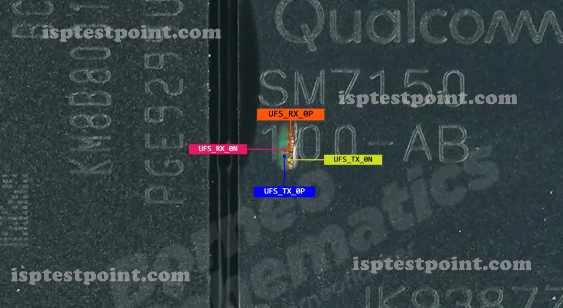
To access the test point on the OPPO Reno 2 CPH1907, you must first fully disassemble the device and remove the motherboard. The CPH1907 uses a Qualcomm Snapdragon 730G platform, and the EDL test point pad is located on the back side of the main PCB. The pad is a small exposed solder point situated near the upper section of the board, in proximity to the Qualcomm SoC. When the correct TP pad is shorted to a neighboring ground pad, it pulls the BOOT_CONFIG line low, signaling the processor to enter EDL mode. Due to component density, use a magnifying lamp or microscope to identify the pad with confidence before attempting contact.
Step-by-Step Access Procedure
Follow these steps carefully to enter EDL mode via test point:
- Power off the device completely and disconnect the battery.
- Disassemble the phone and remove the motherboard from the chassis.
- Identify the EDL test point pad on the rear of the PCB (near the upper SoC area).
- Reconnect the battery carefully, keeping the board accessible.
- Connect a USB cable from the board to your PC running Qualcomm drivers.
- Using a fine-tipped metal tool or pre-made test point wire, short the TP pad to an adjacent ground point.
- While maintaining the short, press and hold the Power button or apply power via the battery connector.
- Release the short after 2–3 seconds. The PC should detect a Qualcomm HS-USB QDLoader 9008 device.
- Launch your flash tool (QFIL, Medusa Pro, EasyJTAG Plus, or UFI Box) and proceed with your intended operation.
Safety Tips and Precautions
Working at the PCB level carries risk of permanent board damage if correct precautions are not observed:
- Always wear an anti-static wrist strap and work on an ESD-safe mat to prevent electrostatic discharge damage to the SoC or UFS storage.
- Use only a fine, insulated probe or dedicated test point wire — never a screwdriver tip that could bridge unintended pads.
- Verify your USB cable and port supply stable 5 V; fluctuating voltage during an active flash operation can corrupt the UFS partition table.
- Do not apply excessive pressure or heat to the PCB while locating pads.
- Always back up IMEI and persist partition data before erasing or rewriting firmware.
Pin / Test Point Reference
| Pin | Description |
|---|---|
| EDL_TP | Test pad shorted to GND to force Qualcomm EDL (9008) mode on power-up — Located on rear side of PCB near upper SoC area; exact pad coordinates unconfirmed — verify under magnification |
Tools required: QFIL (Qualcomm Flash Image Loader), Medusa Pro Box, EasyJTAG Plus, UFI Box, UMT Pro, Qualcomm HS-USB QDLoader 9008 Drivers, Fine-tip test point probe or wire, ESD wrist strap and mat, Magnifying lamp or stereo microscope
Supported operations: FRP Erase, Dead Boot Repair, Firmware Flash (Read/Write), IMEI Repair, Bootloader Unlock, Full eMMC/UFS Backup
⚠ Safety note: Work on ESD-safe surface only. Incorrect pad shorting may cause permanent CPU or UFS damage. Confirm pad location visually before applying power. Voltage must be stable 5 V during flash.

Comments (0)
Be the first to comment.