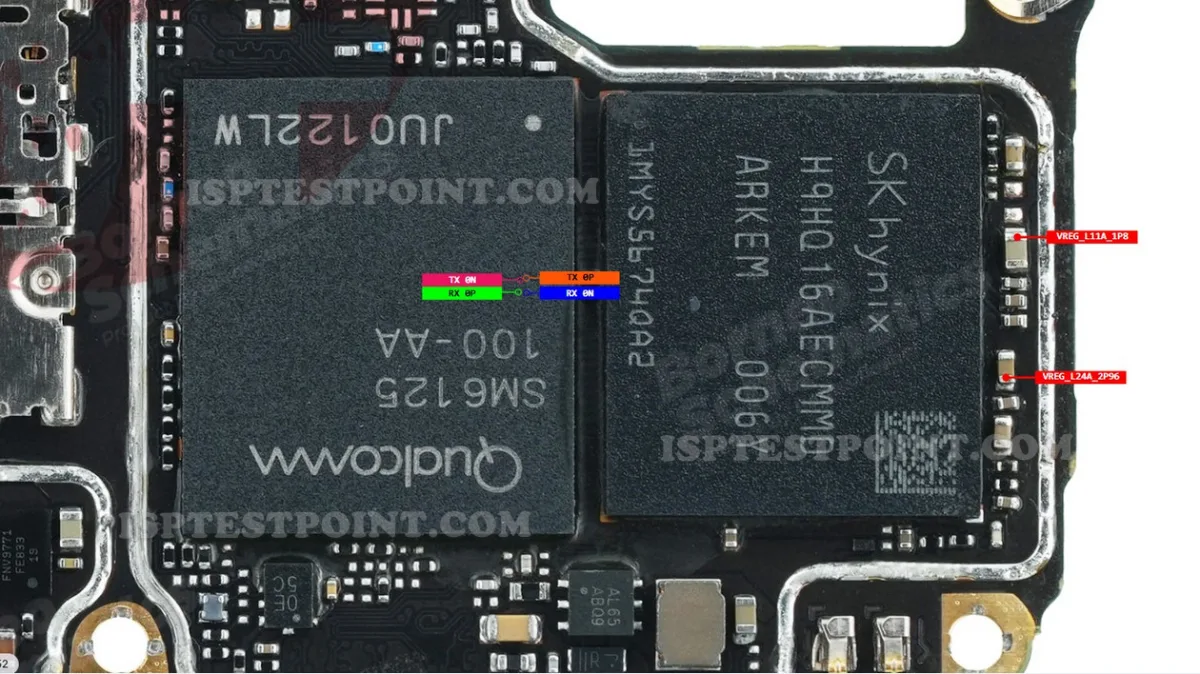
What Is ISP Pinout
ISP (In-System Programming) is a direct hardware method used by mobile repair technicians to communicate with the eMMC flash storage chip on the OPPO A92 CPH2059 PCB without relying on the device's bootloader or operating system. By identifying and connecting to specific test pads on the motherboard, a technician can bypass software locks and access the NAND flash directly. This technique is essential when conventional fastboot, EDL, or ADB-based methods are unavailable or blocked. The OPPO A92 CPH2059 uses an eMMC 5.1 storage interface, and ISP access routes through the eMMC's standard bus lines — CLK, CMD, and DAT0 through DAT7 — along with power (VCC/VCCQ) and ground (GND) connections.

When Technicians Use ISP
ISP is typically chosen when a device has failed beyond the reach of software-based tools. Common scenarios on the OPPO A92 CPH2059 include:
- Device is completely dead or stuck in a boot loop with no EDL or fastboot mode available
- FRP (Factory Reset Protection) lock cannot be bypassed using ADB or third-party APK methods
- The bootloader partition is corrupted and standard flashing tools cannot detect the device
- Screen damage prevents navigation through the UI to initiate a factory reset
- A failed OTA update has left the firmware partition unbootable
In these situations, ISP provides a reliable low-level path to read, write, or erase the eMMC contents directly.
OPPO A92 ISP Test Points
The ISP test pads on the OPPO A92 CPH2059 are located on the back side of the main PCB, typically near the eMMC chip. The standard eMMC bus connections required are listed below. Exact pad coordinates on this specific PCB have not been independently verified in our reference data and are marked uncertain.
- CLK — eMMC clock line
- CMD — eMMC command line
- DAT0–DAT7 — 8-bit data bus lines
- VCC — 3.3 V eMMC core power supply
- VCCQ — 1.8 V eMMC I/O supply
- GND — Common ground reference
Technicians should use a high-resolution PCB diagram specific to the CPH2059 board revision to confirm pad locations before soldering.
Step-by-Step Access Procedure
Follow this procedure carefully to connect your ISP tool to the OPPO A92 CPH2059:
- Power off the device completely and disconnect the battery
- Remove all screws and carefully separate the back panel using a plastic spudger
- Unplug the battery connector and all flex cables from the motherboard
- Remove the motherboard and inspect the back surface under magnification to locate eMMC test pads
- Clean the pads gently with isopropyl alcohol and a soft brush
- Solder fine 30 AWG wires to CLK, CMD, DAT0–DAT7, VCC, VCCQ, and GND pads
- Connect the wires to your ISP tool (e.g., EasyJTAG Plus or UMT ISP adapter)
- Apply controlled power through the tool — do not reconnect the battery during ISP operation
- Launch the appropriate software and select OPPO A92 or the eMMC chip model to begin read/write operations
Safety Tips and Warnings
ISP work on the OPPO A92 CPH2059 involves direct access to sensitive eMMC hardware. Observe the following precautions:
- Never apply more than 3.3 V to VCC or 1.8 V to VCCQ — overvoltage will permanently destroy the eMMC chip
- Double-check every wire connection before powering on; a short between CLK and GND can brick the device instantly
- Use a current-limited bench power supply set to 500 mA or less during ISP operation
- Work in an anti-static environment and use an ESD wrist strap at all times
- Always read (back up) the full eMMC dump before attempting any write or erase operation
- If the eMMC becomes unresponsive mid-operation, do not power cycle abruptly — consult tool documentation for safe abort procedures
Pin / Test Point Reference
| Pin | Description |
|---|---|
| CLK | eMMC clock signal line — Exact pad location not verified; refer to CPH2059-specific PCB diagram |
| CMD | eMMC command line — Exact pad location not verified |
| DAT0 | eMMC data bus bit 0 — Exact pad location not verified |
| DAT1 | eMMC data bus bit 1 — Exact pad location not verified |
| DAT2 | eMMC data bus bit 2 — Exact pad location not verified |
| DAT3 | eMMC data bus bit 3 — Exact pad location not verified |
| DAT4 | eMMC data bus bit 4 — Exact pad location not verified |
| DAT5 | eMMC data bus bit 5 — Exact pad location not verified |
| DAT6 | eMMC data bus bit 6 — Exact pad location not verified |
| DAT7 | eMMC data bus bit 7 — Exact pad location not verified |
| VCC | eMMC core power supply — 3.3 V — Exact pad location not verified |
| VCCQ | eMMC I/O power supply — 1.8 V — Exact pad location not verified |
| GND | Ground reference — Multiple ground points available on PCB |
Tools required: EasyJTAG Plus, UMT ISP Adapter, Medusa Pro II, RIFF Box 2, 30 AWG enameled wire, Soldering station with fine tip, Isopropyl alcohol (90%+), ESD wrist strap, Current-limited bench power supply
Supported operations: Read Full eMMC Dump, Write Firmware, FRP Erase, Dead Boot Repair, IMEI Repair, Pattern/PIN Lock Remove, Bootloader Repair
⚠ Safety note: Do not exceed 3.3V on VCC or 1.8V on VCCQ. Verify all connections before powering on. Always back up full eMMC before any write operation. Work ESD-safe.

Comments (0)
Be the first to comment.