What Is ISP Pinout
ISP (In-System Programming) pinout is a direct hardware method that allows technicians to communicate with a device's eMMC flash chip by probing specific test pads on the printed circuit board. Unlike software-based methods that rely on a functioning bootloader or operating system, ISP bypasses the CPU entirely and connects directly to the eMMC's bus interface. This makes it invaluable when a device cannot boot, has a corrupted partition table, or is locked by FRP (Factory Reset Protection) that cannot be cleared through conventional means. By soldering or probing the correct pads — typically CLK, CMD, DAT0, VCC, VCCQ, and GND — a box or adapter reads and writes the eMMC at the raw data level, enabling full firmware flashing, partition repair, and user data operations.

OPPO A5S CPH1909 ISP Pins
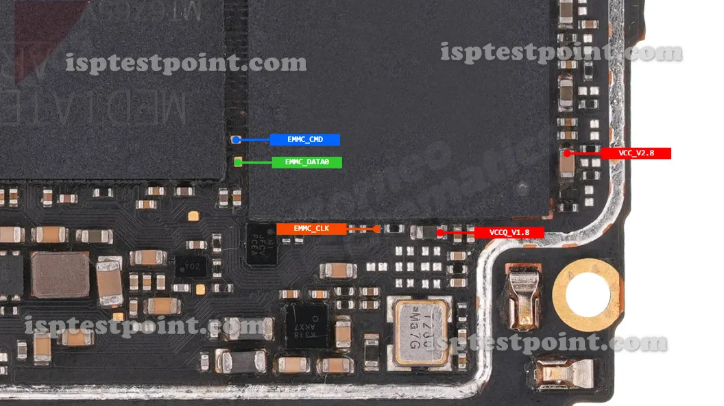
The OPPO A5S CPH1909 uses a MediaTek MT6765 platform with an eMMC 5.1 storage chip. The ISP testpoints are located on the rear side of the main PCB, typically grouped near the eMMC IC. The standard eMMC ISP pins for this device are as follows:
- CLK – eMMC clock signal line
- CMD – Command line for eMMC communication
- DAT0 – Data line 0 (minimum required for ISP read/write)
- VCC – eMMC core power supply (nominally 3.3 V)
- VCCQ – eMMC I/O power supply (nominally 1.8 V)
- GND – Common ground reference
Exact pad coordinates and silk-screen labels on the PCB have not been independently verified for this specific variant. Technicians should cross-reference a verified board diagram or use a multimeter in continuity mode to confirm pad identity before connecting any tool.
When Technicians Use This Method
The ISP method is typically employed when standard USB flashing fails. Common scenarios include: a device stuck in a boot loop after a failed OTA update, a completely dead (no-charge, no-power) device with a suspected corrupt bootloader, pattern lock or FRP that persists after a factory reset attempt, and situations where the download mode or BROM mode is inaccessible due to firmware damage. For the OPPO A5S CPH1909, ISP is also used when SP Flash Tool cannot detect the device through normal USB communication.
How to Access the Testpoints
Follow these steps carefully:
- Power off the device completely and disconnect the battery connector.
- Disassemble the phone and expose the main PCB.
- Identify the eMMC IC and locate the six ISP testpoints using a board schematic or verified reference image.
- Solder thin gauge (30–32 AWG) wires or use a quality ISP probe/clip to each pad — CLK, CMD, DAT0, VCC, VCCQ, and GND.
- Connect wires to your ISP adapter (e.g., EasyJTAG Plus eMMC socket or UMT ISP adapter).
- Launch your tool software, select the MediaTek eMMC platform, and power the eMMC via the tool's regulated supply.
- Initiate a full dump, targeted partition read, or FRP erase as required.
Safety Tips and Precautions
Working at eMMC level carries significant risks. Always observe the following precautions:
- Never apply more than 3.3 V to VCC or 1.8 V to VCCQ — overvoltage permanently destroys the eMMC.
- A full ISP read will erase or overwrite user data; inform the customer before proceeding.
- Using an incorrect pinout can short-circuit the board — always verify with continuity checks first.
- Use temperature-controlled soldering equipment and work quickly to avoid PCB pad lifting.
- Back up the full eMMC dump before performing any write operation.
Pin / Test Point Reference
| Pin | Description |
|---|---|
| CLK | eMMC clock signal — Exact PCB pad location unverified — confirm with continuity check |
| CMD | eMMC command line — Exact PCB pad location unverified — confirm with continuity check |
| DAT0 | eMMC data line 0 — Minimum required data line for ISP operation |
| VCC | eMMC core power supply (~3.3 V) — Do not exceed 3.3 V |
| VCCQ | eMMC I/O power supply (~1.8 V) — Do not exceed 1.8 V |
| GND | Ground reference — Multiple GND pads usually available near eMMC |
Tools required: EasyJTAG Plus with eMMC ISP adapter, UMT (Ultimate Multi Tool) with ISP cable, Medusa Pro II, UFI Box, 30–32 AWG magnet wire, Temperature-controlled soldering station, Multimeter (for continuity verification)
Supported operations: Read Full eMMC Dump, Write Full eMMC Dump, FRP Erase, Dead Boot Repair, Firmware Flash, Partition Repair, Pattern/PIN Lock Remove
⚠ Safety note: VCC max 3.3 V, VCCQ max 1.8 V. Wrong pinout may permanently damage the eMMC or PCB. Always back up before writing. Operation erases user data.

Comments (0)
Be the first to comment.