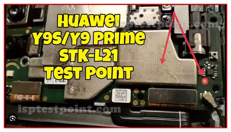
What Is a Test Point
A test point is a designated conductive pad exposed on a device's printed circuit board (PCB) that allows technicians to communicate directly with the chipset or storage, bypassing normal software boot sequences. On the Huawei Y9S, test points are critical for low-level operations such as forcing the device into a flash-friendly state, erasing FRP locks, or recovering a board that refuses to power on. Because Huawei devices use HiSilicon chipsets with proprietary boot protocols, physical test point access is often the only reliable path when software-based tools fail.

When Technicians Need This
Test point access on the Huawei Y9S becomes necessary in several common repair scenarios:
- FRP (Factory Reset Protection) bypass — when a second-hand device is locked to a previous Google account and software unlock methods are exhausted.
- Dead boot recovery — when a failed firmware update or corrupt partition leaves the device unable to power on or reach fastboot.
- ISP (In-System Programming) flashing — when the USB port is damaged or the device no longer enumerates over USB, requiring direct eMMC/UFS access via pads.
- Bootloader unlock preparation — in certain advanced scenarios requiring low-level partition manipulation.
Locating the Test Points
The Huawei Y9S PCB test pads are located on the back side of the main board, typically near the UFS storage chip. After removing the rear cover and disconnecting the battery, the primary ISP pads (CLK, CMD, DAT0, VCC, GND, and VCCQ) are clustered in the lower-mid section of the board close to the eMMC/UFS package. A secondary GND short pad used to trigger download mode is found near the CPU area. Due to the compact form factor of the Y9S, a magnifying lens (10x or higher) is recommended to precisely identify each pad before probing. Always cross-reference with a verified PCB diagram before making contact.
Step-by-Step Access Procedure
Follow these steps carefully to access the Y9S test point mode:
- Power off the device completely and remove the SIM tray.
- Apply controlled heat (70–80 °C) to the rear glass panel and pry it off gently using a plastic spudger.
- Remove all visible screws securing the mid-frame and carefully lift the PCB assembly.
- Disconnect the battery flex cable immediately to prevent accidental boot.
- Identify the GND test pad and the target ISP pads using a PCB diagram or multimeter continuity check.
- Connect your ISP adapter or wire leads to the appropriate pads (CLK, CMD, DAT0, GND, VCC, VCCQ).
- Launch your flashing tool (e.g., EasyJTAG Plus or UFI Box), select the correct pinout, and power the board via tool supply.
- Execute the desired operation — read, write, or erase — and disconnect cleanly when complete.
Safety Tips and Warnings
Working at the PCB level carries significant risk. Observe these precautions:
- Always disconnect the battery before probing any test pad to avoid short circuits.
- Use 1.8 V logic levels for UFS pads — applying 3.3 V will permanently damage the storage chip.
- Never apply heat directly to the PCB; use controlled warm air on the chassis only.
- Double-check pad continuity with a multimeter before powering the board through a test jig.
- Work in an ESD-safe environment with a grounding strap to protect sensitive HiSilicon components.
- Attempt ISP procedures only if USB-based recovery has been fully exhausted.
Pin / Test Point Reference
| Pin | Description |
|---|---|
| CLK | UFS clock signal pad for ISP access — 1.8 V logic — verify before connecting |
| CMD | UFS command line pad — 1.8 V logic |
| DAT0 | UFS data line pad (primary data channel) — 1.8 V logic |
| VCC | Storage power supply pad (2.7–3.6 V for UFS core) — Confirm voltage with tool specs |
| VCCQ | UFS I/O voltage supply pad (1.8 V) — Critical — do not exceed 1.8 V |
| GND | Ground reference pad — Multiple GND pads available near PCB edge |
| GND Short Pad | Short to GND with USB connected to trigger download/flash mode — Exact pad location uncertain — verify with PCB diagram |
Tools required: EasyJTAG Plus, UFI Box, UMT Dongle, Medusa Pro II, ISP adapter/jig for UFS, Multimeter, Hot air station, Plastic spudger set, ESD wrist strap
Supported operations: FRP Erase, Dead Boot Repair, Read Firmware, Write Firmware, IMEI Repair, Full eMMC/UFS Backup, Partition Erase
⚠ Safety note: Use 1.8 V only on UFS I/O pads. Disconnect battery before probing. Incorrect voltage will permanently destroy the UFS storage chip.

Comments (0)
Be the first to comment.