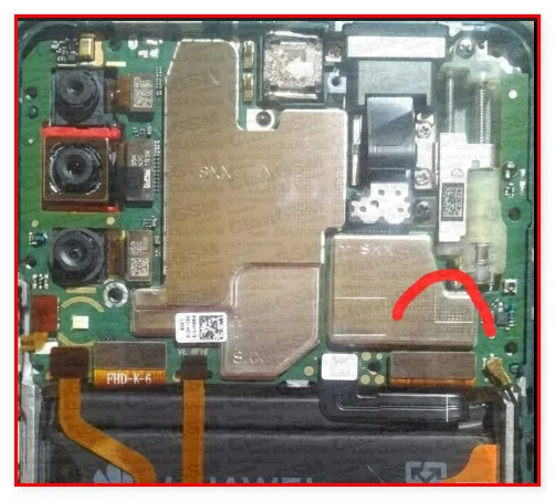
Test Point Overview
The Huawei Y9 Prime 2019 (STK-LX3) is a mid-range Android smartphone powered by the Snapdragon 665 processor. Test points on this device provide direct access to hardware diagnostics, firmware flashing, and factory recovery modes. These dedicated pads allow technicians to bypass software locks, restore corrupted partitions, and perform emergency boot repairs without relying on functional USB connectivity or software interfaces.

When to Use Test Points
Hardware test points are essential when the device exhibits critical failures:
- FRP (Factory Reset Protection) lock bypass when standard unlocking fails
- Complete dead-boot scenarios with no power-on response or stuck boot loops
- Corrupted firmware requiring emergency reflash via eMMC direct access
- Unresponsive USB detection or download mode failures
- Security partition corruption preventing normal factory reset
Direct test point access circumvents software protections and enables recovery when standard troubleshooting cannot restore functionality.
Access Procedure
Accessing test points requires precision and proper equipment:
- Power off the device completely and remove the battery (if user-removable)
- Locate the mainboard and identify test pad clusters near the processor and eMMC chip
- Connect appropriate ISP cables (UMT or EasyJTAG compatible) to designated test pads with correct polarity
- Establish stable connections using fine-tip probes or pogo-pin adapters
- Load correct firmware bins and partition files into your flashing tool
- Follow tool-specific flashing sequences without interrupting power or data transfer
Key Test Points Location
Test point locations on the STK-LX3 mainboard are distributed across functional zones. Primary eMMC access pads are typically clustered near the storage IC on the rear of the motherboard. CPU-related diagnostics pads are positioned adjacent to the Snapdragon 665 chipset. Precise coordinates and individual pad names vary by board revision; consult your device's specific board schematic for exact TP locations. Ground reference pads are abundant around the board perimeter for stable probe attachment.
Safety Precautions
Working with exposed test points carries electrical and mechanical risks. Always use an anti-static wrist strap and work on a grounded surface to prevent ESD damage. Verify voltage levels (typically 3.3V for digital signals) before connecting any external equipment. Never apply power while probes or adapters are partially seated; ensure all connections are fully established first. Avoid excessive pressure on delicate pads to prevent copper trace separation. If the device is powered during operations, disconnect immediately if unusual heat or smoke appears. Back up all firmware before any reflash operation. Test points bypass security mechanisms—use this capability only on devices you own or are authorized to service.
Pin / Test Point Reference
| Pin | Description |
|---|---|
| GND | Ground reference pad(s), typically multiple locations around mainboard periphery — Essential for probe stability and measurement reference |
| VCC / VCCQ | Primary power supply and I/O voltage rails for eMMC and processor — Typically 3.3V digital, verify before connection |
| CLK | eMMC clock signal test point — Part of eMMC ISP interface |
| CMD | eMMC command signal test point — Part of eMMC ISP interface |
| DAT0–DAT7 | eMMC data bus test points (8-bit wide) — Critical for firmware read/write operations |
| RST / RSTB | eMMC reset signal pad — Controls eMMC reset state during ISP operations |
Tools required: UMT (Universal Micro Tool) with STK-LX3 support, EasyJTAG Plus or compatible eMMC programmer, Fine-tip soldering iron or pogo-pin test probe adapter, Multimeter for voltage verification, Anti-static wrist strap and grounded work surface, STK-LX3 firmware bins and partition files
Supported operations: Read Full Firmware Dump, Write / Reflash Firmware Partitions, FRP Unlock via Security Partition Erase, Dead Boot Repair (Emergency Flash), Bootloader Bypass, eMMC Direct Access and Verification
⚠ Safety note: HIGH VOLTAGE RISK: Do not connect test points while device is powered with wall charger. Snapdragon 665 core voltages and memory rails carry 1.8–3.3V; miswired connections may cause permanent IC damage. Always discharge static electricity and ground work area. Probe contact errors can short signal lines—fatal to mainboard.

Comments (0)
Be the first to comment.