Overview
The Huawei Y9 2019 (JKM-LX1) is a mid-range Android device featuring the Kirin 710 processor and a dual-camera setup. Test points on this device provide direct access to the eMMC storage and system firmware, enabling technicians to perform FRP (Factory Reset Protection) bypass, firmware restoration, and emergency boot recovery. These hardware-level access points are essential when software methods fail or the device enters a bootloop state. Proper identification and safe probing of test points ensure successful data recovery and device restoration without damaging sensitive components.

When to Use Test Points
Test points should be used in the following diagnostic scenarios: device stuck in bootloop or boot failure, FRP lock requiring password recovery, corrupted firmware or system partitions, dead battery with no USB detection, complete software brick, and password-locked accounts preventing factory reset. These points bypass software security layers and allow direct firmware read/write operations. Test point access is appropriate only when conventional recovery methods (recovery mode, EDL, fastboot) have been exhausted. Always verify the device is non-functional via standard methods before proceeding with hardware probing.
Common Test Point Locations
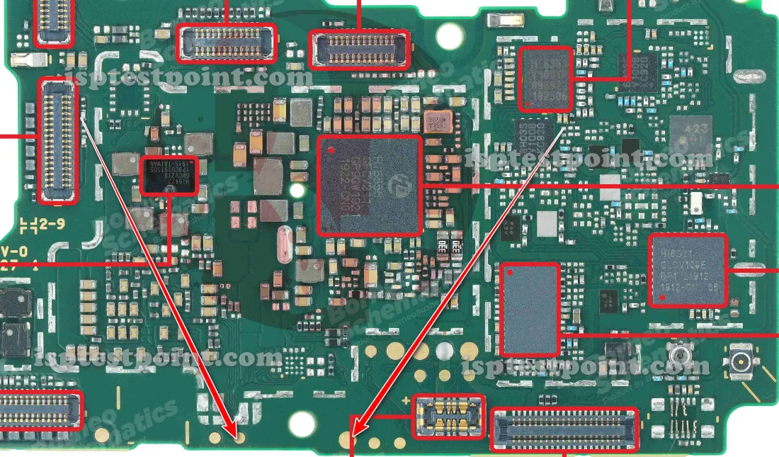
The primary test points on the Huawei Y9 2019 are located on the main logic board near the eMMC storage chip and power management IC. The eMMC test pad cluster typically occupies a small area adjacent to the storage module, containing CMD, CLK, DAT0-DAT3, VCC, GND, and RST signals. Additional test points exist for USB boot entry (short-to-ground activation) and battery connection verification. Exact pad coordinates and silk-screen labels vary by PCB revision; reference high-resolution board photography and schematic diagrams specific to JKM-LX1 hardware revision before attempting contact.
Access Procedure
Remove the device back cover and disconnect the battery to prevent accidental short circuits. Locate the main logic board and identify the eMMC storage chip near the processor area. Using a magnifying glass and fine-tip probe, carefully contact each test pad while the device is powered down. Connect ISP hardware (UMT Box, Riff Box, or compatible eMMC reader) to the test points in the correct sequence: VCC first, then CMD, CLK, DAT0, RST, and GND last. Verify all connections with a multimeter before applying power. Power on the ISP box and launch appropriate flashing software to detect the eMMC chip. Avoid excessive pressure on pads to prevent circuit damage.
Safety Precautions
Always disconnect the battery before accessing test points to prevent accidental shorts and component damage. Use insulated fine-tip probes and avoid simultaneous contact with adjacent pads. Verify ISP box voltage output matches eMMC specifications (typically 3.3V). Do not apply power while probes are loose or misaligned. Ground yourself properly to discharge static electricity. Allow the device to cool before handling after extended testing. Never probe test points while the device is powered on via USB or battery. If uncertain about pad identification, consult high-resolution board schematics or request clarification from experienced technicians before proceeding.
Pin / Test Point Reference
| Pin | Description |
|---|---|
| CLK | eMMC clock signal — Connect to ISP box CLK line |
| CMD | eMMC command signal — Bidirectional data command line |
| DAT0 | eMMC data line 0 — Primary data transfer |
| VCC | eMMC power supply (+3.3V) — Connect first, verify voltage |
| GND | Ground reference — Connect last for safety |
| RST | eMMC reset signal — Active-low reset control |
Tools required: UMT Box or Riff Box, eMMC ISP reader, Fine-tip multimeter probes, Magnifying glass (10x minimum), Insulated tweezers, Thermal paste (for reassembly)
Supported operations: Read Firmware, FRP Erase/Bypass, Dead Boot Repair, eMMC Full Backup, Partition Restore, Bootloader Access
⚠ Safety note: 3.3V eMMC interface — verify ISP box output. Disconnect battery before probing. Static-sensitive components present. Do not apply power with loose probe connections. Device may become unusable if test points are damaged.

Comments (0)
Be the first to comment.