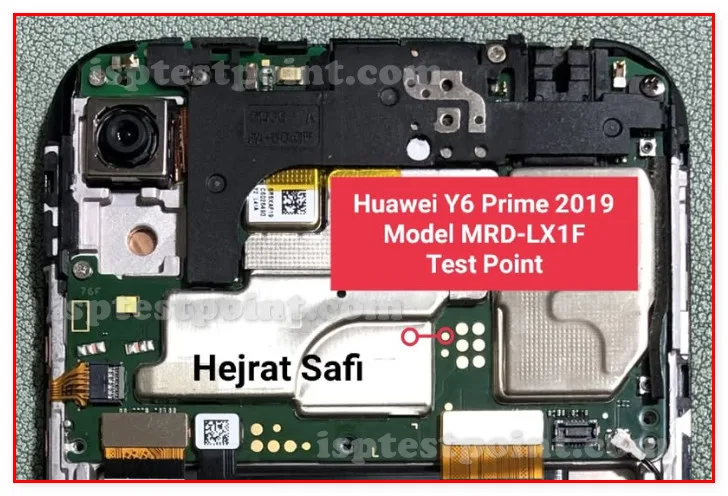
Overview — Test Point Access Fundamentals for Y6 2019 Hardware Diagnosis
The Huawei Y6 2019 (MRD-LX1F) is a budget-segment device built on Mediatek MT6761 (Helio A22) architecture. Test points on this model enable direct eMMC communication for firmware recovery, FRP (Factory Reset Protection) removal, and dead-boot restoration without requiring functional software pathways. The mainboard layout follows standard Mediatek reference designs, with eMMC test pads clustered near the storage IC on the lower-left section of the logic board.
Accessing test points requires disassembly to the mainboard level and careful micro-soldering or spring-probe contact to exposed test pads. Understanding voltage levels (1.8V eMMC signaling) and clock/data line topology is essential for safe operation.

When to Use Test Points — Common Failure Scenarios Requiring Test Point Verification
Test point access becomes necessary when:
- FRP Lock: Device boots but demands Google Account verification after factory reset.
- Dead Boot / No Signal: Device does not respond to USB or produces no output; software recovery impossible.
- Corrupted Firmware: Bootloader or system partition damaged; standard flashing tools fail to communicate.
- Baseband/Modem Issues: Complete loss of network registration or baseband crashes.
- eMMC Communication Failure: Storage IC unresponsive to standard protocol; ISP mode required.
In these scenarios, ISP (In-System Programming) via test points bypasses the device OS entirely, allowing direct read/write access to flash memory.
Access Procedure — Step-by-Step Navigation to Locate and Probe Test Points Safely
Disassembly: Remove back cover and battery (non-removable; disconnect flex connector). Unscrew mainboard from frame; carefully lift logic board away from antenna flex cables.
Test Pad Location: Orient mainboard with USB port facing downward. eMMC test pads are typically positioned on the lower-left quadrant, adjacent to or beneath the storage IC. Use magnification (10–20×) to identify tiny copper pads labeled CLK, CMD, DAT0, VCC, GND, VCCQ, and RST. Exact pad locations are device-revision dependent; schematic reference is strongly recommended.
Probing Method: Spring-probe ISP clips or micro-soldering are the two common approaches. For temporary work, fine-gauge wire (36–40 AWG) soldered to test pads with low-temperature solder is acceptable. Ensure all probes contact the pad center; avoid bridging adjacent pads.
Safety Precautions — Essential Grounding and Voltage Awareness for Technician Protection
Static Discharge (ESD): Always wear an anti-static wristband connected to a grounded mat. Ground yourself before touching the mainboard or test points.
Voltage Awareness: eMMC operates at 1.8V; exposing 3.3V or higher logic to eMMC data lines causes irreversible damage. Verify tool/adapter voltage output before connection.
Power State: Never probe test points while the device is powered on or connected to USB. Disconnect battery flex entirely.
Soldering Safety: Use a temperature-controlled soldering iron (≤350°C) with fine-tip heating elements. Avoid prolonged heat exposure near the storage IC; adjacent capacitors and resistors may desolder or burn.
Tool Calibration: Test ISP software (UMT, EasyJTAG, or MtkClient) on a known-good device before attempting repair on the target unit.
Pin / Test Point Reference
| Pin | Description |
|---|---|
| CLK | eMMC clock signal — 1.8V signaling |
| CMD | eMMC command/response line — 1.8V signaling |
| DAT0 | eMMC data line 0 (or DAT0–DAT3 for 4-bit mode) — Primary data lane |
| VCC | eMMC core power (1.8V) — Verify regulated supply |
| VCCQ | eMMC I/O power (1.8V) — Separate from VCC |
| GND | Ground reference — Multiple pads; contact all available |
| RST | eMMC hardware reset (active-low) — Optional; some tools do not require |
Tools required: UMT (Uni_Meta Tool) or EasyJTAG Plus, MtkClient (open-source alternative), Spring-probe ISP clip or micro-soldering equipment, Temperature-controlled soldering iron (≤350°C), Multimeter (voltage verification), Anti-static wristband and ESD mat, Magnification lens (10–20×), Fine-gauge wire (36–40 AWG) or solder bridge jumpers
Supported operations: Read Full Firmware, Write Full Firmware, FRP Erase, Dead Boot Repair, Baseband/Modem Recovery, eMMC Chip Dump, Partition-Level Flashing
⚠ Safety note: eMMC operates at 1.8V — never apply 3.3V or higher logic signals. Always disconnect battery and ground yourself before probing. Soldering near storage IC risks thermal damage to adjacent components.

Comments (0)
Be the first to comment.