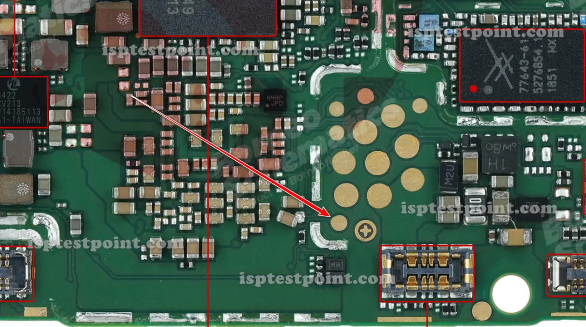
Overview
The Huawei P30 Lite is a mid-range smartphone equipped with a Kirin 710 processor and eMMC 5.1 storage. Test points on the P30 Lite motherboard provide direct access to the eMMC memory for firmware operations, including flashing custom ROMs, erasing FRP (Factory Reset Protection), and recovering from dead-boot conditions. These test pads enable technicians to bypass software locks and perform low-level diagnostics when standard recovery methods fail.

Common Test Point Locations
The eMMC test points on the Huawei P30 Lite are located on the rear of the main motherboard, positioned near the storage IC. Key access points include:
- CLK (Clock): Controls timing signals for memory operations
- CMD (Command): Carries command and address data
- DAT0–DAT3: Data bus lines for read/write operations
- VCC/VCCQ: Power supply pins (3.3V nominal)
- GND: Ground reference points (multiple locations)
- RST: Reset signal line
USB-to-eMMC bridge adapters provide convenient access without requiring micro-soldering when factory test pads are exposed.
When to Use Test Points
Test points are essential in the following scenarios:
- Device enters bootloop or dead-boot state
- FRP lock prevents activation after factory reset
- Corrupted bootloader prevents normal startup
- Firmware flashing via Huawei's HiSuite or third-party tools fails
- Emergency recovery when device is unresponsive to standard adb/fastboot commands
Huawei Test Point All Models Download
Access and Measurement Procedure
Before beginning, ensure the device is powered off and the battery is removed. Using a multimeter set to continuity mode, identify test pads by tracing connections from the eMMC IC to accessible solder points on the motherboard. Connect a UMT box or equivalent eMMC reader via USB to the test points using fine jumper wires or pogo pins. Secure connections with minimal pressure to avoid damaging delicate traces. Power the device via USB and allow the flashing software to detect the eMMC. Follow manufacturer-specific instructions for your tool (UMT, EasyJTAG, etc.) to read, erase, or write firmware images. Verify successful operations through log files before reassembling the device.
Safety Precautions
Never apply voltages exceeding 3.6V to eMMC pins—damage to storage is irreversible. Remove the battery before probing to prevent accidental short circuits. Use ESD protection mats and wrist straps when handling the motherboard. Keep test points free from moisture and contamination. If uncertain about pin identification, consult high-resolution board images or reference schematics. Always test continuity before connecting power. Avoid prolonged probe contact that may cause corrosion or pad lift.
Pin / Test Point Reference
| Pin | Description |
|---|---|
| CLK | eMMC clock signal — Connect to CLK line on eMMC reader |
| CMD | eMMC command/address bus — Bidirectional data line |
| DAT0 | eMMC data line 0 — Primary data signal |
| DAT1 | eMMC data line 1 — Secondary data signal |
| DAT2 | eMMC data line 2 — Secondary data signal |
| DAT3 | eMMC data line 3 — Secondary data signal |
| VCC | eMMC primary power supply — 3.3V nominal |
| VCCQ | eMMC I/O power supply — 3.3V nominal |
| GND | Ground reference — Multiple points on board |
| RST | eMMC reset signal — Active low |
Tools required: UMT Box, EasyJTAG Plus, Huawei eMMC Reader (USB-based), Fine jumper wires or pogo pin connector, Multimeter (continuity mode), ESD protection mat and wrist strap, Micro-soldering equipment (optional for pad repair)
Supported operations: Read Firmware, Write Firmware, Erase eMMC, FRP Unlock, Dead Boot Repair, Bootloop Recovery
⚠ Safety note: Do not exceed 3.6V on eMMC pins. Remove battery before probing. Use ESD protection. Incorrect connections may permanently damage eMMC storage. Proceed only if you have experience with eMMC-level repair.

Comments (0)
Be the first to comment.