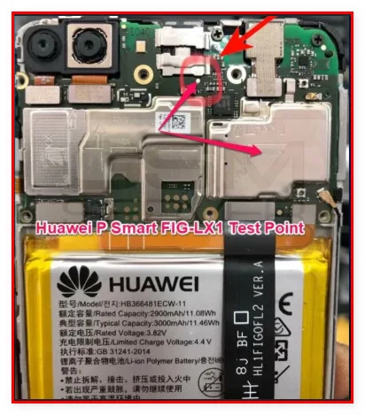
What Are Test Points — Essential Diagnostic Connection Locations on the Device PCB for Technicians
Test points are small copper pads or via holes soldered directly to the device's main circuit board (PCB). They provide direct access to critical signal lines including eMMC data lines, clock signals, power rails, and ground planes. For the Huawei P Smart Fig-LX1, test points enable technicians to bypass software locks and communicate directly with the storage chip when standard boot methods are unavailable. These connection points are typically 0.5–1.5 mm in diameter and require precision soldering equipment to access safely.

When to Use Test Points — Required When Standard Boot Methods Fail or for Advanced Troubleshooting
Test points become necessary when the device exhibits dead-boot conditions, fails to enter download mode, or displays persistent FRP (Factory Reset Protection) locks that prevent normal unlocking procedures. Common scenarios include corrupted bootloader firmware, failed OTA updates, or devices with inaccessible recovery partitions. Technicians use test point connections to read the raw eMMC memory, reflash the bootloader, or erase FRP data directly, restoring functionality without relying on the device's operating system.
Common Test Point Locations — Reference Map of Ground, Power, and Signal Points on Fig-LX1
The Huawei P Smart Fig-LX1 features eMMC test points clustered near the storage chip, typically located on the lower half of the motherboard. Standard eMMC interface pads include CLK (clock), CMD (command), DAT0–DAT3 (data lines), VCC (3.3V power), VCCQ (1.8V I/O voltage), GND (ground), and RST (reset). Ground pads are distributed across the PCB for stability. Exact pad coordinates vary slightly by hardware revision; cross-reference your specific device variant before attempting access. Power and signal test points are often color-coded on the PCB or marked with silk-screen labels.
Safe Access Procedure — Step-by-Step Method for Connecting Test Equipment Without Damaging Components
- Power off the device completely and disconnect the battery before proceeding.
- Use a precision microscope (10–40× magnification) to locate and identify test pads.
- Apply a small amount of flux to each test pad to improve solder adhesion.
- Use a fine-tipped soldering iron (25–40W) to attach thin gauge wire (32–36 AWG) to each pad, holding contact for 2–3 seconds per connection.
- Double-check wire routing to prevent shorts between adjacent pads.
- Connect the opposite wire ends to your programming equipment (UMT, EasyJTAG) following the tool's pin-out diagram.
- Verify all connections are stable before powering on the device or connecting USB.
Safety Precautions — Critical Warnings to Prevent Short Circuits, Data Loss, and Hardware Damage
Never apply voltage to test points while the device is powered on. Always verify correct polarity and voltage levels (3.3V vs. 1.8V) before connecting equipment. Short circuits between adjacent pads can permanently damage the eMMC or CPU. Use insulated tools and avoid contact with live components. Ensure proper grounding of your workstation to prevent electrostatic discharge (ESD). Back up any recoverable firmware before attempting repairs. If uncertain about pad identification, consult multi-angle high-resolution images or professional repair documentation specific to your hardware revision.
Pin / Test Point Reference
| Pin | Description |
|---|---|
| CLK | eMMC clock signal; typically near storage chip — 3.3V logic level |
| CMD | eMMC command/data line for device communication — 3.3V logic level |
| DAT0 | Primary eMMC data line — 1.8V I/O on some variants |
| DAT1 | Secondary eMMC data line — 1.8V I/O on some variants |
| DAT2 | Tertiary eMMC data line — 1.8V I/O on some variants |
| DAT3 | Quaternary eMMC data line; may serve as chip select — 1.8V I/O on some variants |
| VCC | Primary power supply for eMMC (3.3V) — Do not exceed 3.6V |
| VCCQ | I/O power supply for eMMC (1.8V typical) — Voltage depends on device variant |
| GND | Ground reference; multiple pads across PCB — Essential for stable signal integrity |
| RST | eMMC reset signal for hardware reset — Active low; typically pulled high via resistor |
Tools required: UMT (Universal Multi Tool), EasyJTAG Plus, Precision soldering iron (25–40W), Fine-gauge wire (32–36 AWG), Flux pen, Microscope (10–40× magnification), Multimeter, Anti-static wrist strap
Supported operations: Read Firmware, Write Firmware, FRP Erase, Bootloader Repair, Dead Boot Repair, eMMC Direct Access
⚠ Safety note: Do not apply voltage to test points while device is powered on. Verify correct voltage levels (3.3V vs. 1.8V) before connection. Short circuits between adjacent pads can permanently damage eMMC or CPU. Ensure proper ESD grounding. Back up firmware before attempting repairs.

Comments (0)
Be the first to comment.