Overview
The Huawei Nova Y70 Plus is a budget-range smartphone built on the MediaTek Helio G35 platform. Test points provide direct access to critical voltage rails, ground planes, and signal lines necessary for firmware diagnostics, FRP (Factory Reset Protection) bypass, and emergency boot repair. These diagnostic pads are essential when standard USB recovery methods fail or the device enters a bricked state. Understanding the location and function of each test point enables technicians to safely perform ISP (In-System Programming) operations and validate hardware integrity during troubleshooting.

When to Use Test Points
Test point access becomes necessary in several failure scenarios: device enters a bootloop or dead-boot condition; FRP lock requires bypass without losing data; firmware corruption prevents normal recovery through USB; battery or charging circuit issues require voltage rail diagnostics; or when the boot ROM is inaccessible via standard methods. Technicians typically resort to test points when the device does not respond to recovery mode shortcuts or when UMT/EasyJTAG tools fail to establish communication through normal interfaces. These points allow direct hardware-level intervention independent of software state.
Accessing Test Points
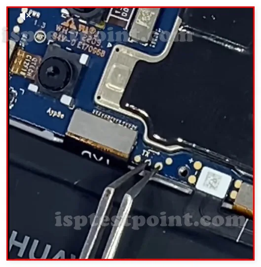
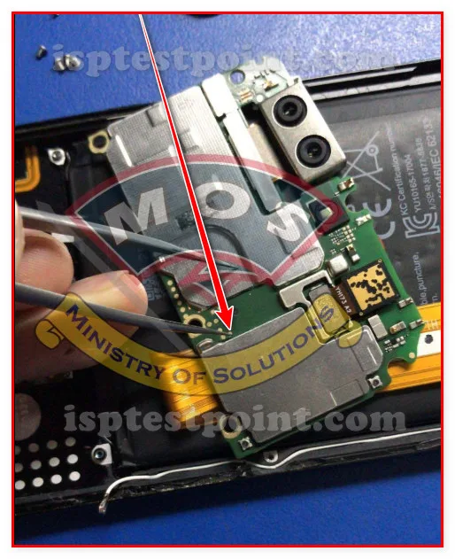
Begin by removing the device back cover and locating the main PCB. Test points on the Nova Y70 Plus are typically clustered near the CPU and power management IC (PMIC) areas. Use a magnifying glass or digital microscope to identify small solder pads marked with silkscreen labels or arranged in recognizable patterns. Carefully tin each test pad with a thin wire or pogo probe to ensure reliable contact. Connect your ISP programmer (UMT, EasyJTAG Plus, or equivalent) according to the pin mapping. Secure the probe assembly with a stable jig or holders to prevent intermittent contact during read/write operations. Always verify continuity with a multimeter before attempting any firmware operation.
Key Test Points Reference
Critical diagnostic points include: GND (ground reference for all measurements), VBAT (main battery voltage, typically 3.7–4.2 V), VDD_CORE (CPU core supply, ~0.8–1.0 V), VDDQ (memory IO supply, ~1.8 V), and CLK/CMD/DAT signal lines for eMMC or UFS communication. The exact pad locations and voltage thresholds vary based on PCB revision. Boot mode selection pins (if accessible) may allow forced entry into EDL (Emergency Download Mode) or Qualcomm-style diagnostic mode. Consult the specific board schematic or PCB topology to map signal integrity test points.
Safety Precautions
Always disconnect the battery before probing test points to prevent short-circuit damage. Use ESD-safe equipment and grounding straps. Never apply external voltage exceeding rated rail specifications—overvoltage will permanently damage ICs. When using pogo probes, apply minimal downward force to avoid tearing fragile solder pads. Do not attempt test point work on devices with visible water damage or corrosion without thorough cleaning. Ensure your ISP programmer firmware supports the Nova Y70 Plus chipset and architecture before connecting.
Pin / Test Point Reference
| Pin | Description |
|---|---|
| GND | Ground reference point; used as baseline for all voltage measurements and probe grounding. — Multiple GND pads available on PCB |
| VBAT | Main battery supply rail, typically 3.7–4.2 V DC. — Verify before boot attempt |
| VDD_CORE | CPU core voltage supply, approximately 0.8–1.0 V. — Critical for CPU operation |
| VDDQ | Memory IO voltage supply, typically 1.8 V. — Regulates eMMC/UFS interface |
| CLK | eMMC/UFS clock signal line. — Essential for memory communication |
| CMD | eMMC/UFS command signal line. — Data protocol control |
| DAT0 | eMMC/UFS data line 0. — Primary data bus line |
Tools required: UMT (Universal Modification Tool), EasyJTAG Plus, Digital Multimeter, Magnifying Glass or USB Microscope, Pogo Probe Set or ISP Test Clip, ESD-Safe Soldering Iron (for pad repair), Schematic Diagram for Nova Y70 Plus
Supported operations: Read Firmware, Write Firmware, FRP Erase, Dead Boot Repair, Voltage Rail Testing, EDL/Diagnostic Mode Entry
⚠ Safety note: High risk of permanent IC damage if incorrect voltage applied. Disconnect battery before probing. Use ESD protection. Do not exceed rated voltage specifications (core: ~1.0 V max, IO: ~1.8 V max). Bricked devices may have damaged power circuits—validate voltage rails before powering on.

Comments (0)
Be the first to comment.