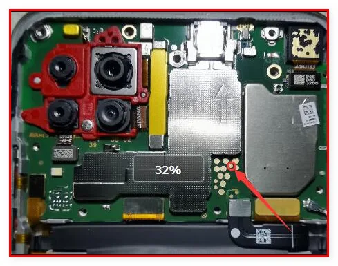
What Is a Test Point
A test point is a designated pad or exposed copper contact on a device's printed circuit board (PCB) that allows technicians to establish a direct electrical connection for diagnostic and recovery operations. On the Huawei Nova 7i JNY-LX2, test points are used to force the device into a special communication mode — bypassing normal boot sequences — so that firmware can be written, FRP locks can be cleared, or a bricked device can be recovered. These pads are intentionally left accessible by manufacturers for factory-level testing and are essential tools in professional mobile repair workflows.

When Technicians Need This
There are several common scenarios where accessing the test point on the Huawei Nova 7i JNY-LX2 becomes necessary:
- FRP (Factory Reset Protection) bypass: When a device is locked to a Google account after a hard reset and the credentials are unavailable.
- Dead boot repair: When the phone fails to power on due to a failed OTA update, interrupted flash, or corrupted bootloader.
- Firmware flashing: When standard ADB/fastboot methods are inaccessible and direct UFS communication is required.
- IMEI repair: In cases where the IMEI has been corrupted and needs to be restored via direct board access.
- Bootloop recovery: When the device continuously restarts without completing the boot sequence.
Locating the Test Point
The Huawei Nova 7i JNY-LX2 uses a UFS 2.1 storage chip paired with the HiSilicon Kirin 810 SoC. For ISP (In-System Programming) access, technicians must identify the UFS test pads on the motherboard. These pads correspond to the UFS interface signals. The primary test point used to trigger the download or recovery mode is typically located near the UFS IC on the back side of the main PCB. After removing the rear cover and disconnecting the battery, inspect the board surface under magnification for labeled or unlabeled solder pads near the storage controller area.
Note: Exact pad coordinates and silkscreen labels for the JNY-LX2 variant have not been universally confirmed across repair sources. Technicians should cross-reference with a verified PCB diagram or board schematic before probing.
Step-by-Step Access Procedure
Follow these steps carefully to access the test point on the Huawei Nova 7i JNY-LX2:
- Power off the device completely and remove the SIM tray.
- Use a heat gun to warm the rear panel edges, then carefully pry it open with a suction cup and spudger.
- Disconnect the battery flex connector from the motherboard immediately.
- Locate the UFS ISP pads on the PCB using a magnifier or microscope.
- Solder or use a spring-pin ISP adapter to connect CLK, CMD, DAT0, VCC, GND, and VCCQ lines to your programmer.
- Connect the programer (e.g., EasyJTAG Plus or UFi Box) to your PC and launch the appropriate software.
- Apply power through the tool and initiate the desired operation (read, erase, or write).
Safety Tips and Precautions
Working at the PCB level carries significant risk. Observe the following precautions:
- Always disconnect the battery before probing any test pads to prevent short-circuit damage.
- Use a regulated power supply if powering the board externally — overvoltage will permanently damage the Kirin 810 SoC or UFS chip.
- Avoid applying excessive heat to the board when soldering to ISP pads; use fine-tip soldering irons at controlled temperatures.
- Ground yourself with an anti-static wrist strap before handling the PCB.
- Double-check pin assignments before powering on — reversed VCC and GND will destroy the storage IC instantly.
- Always back up the current firmware before performing any write or erase operation.
Pin / Test Point Reference
| Pin | Description |
|---|---|
| CLK | UFS clock signal pad for ISP programming — Exact pad location unconfirmed; verify with schematic |
| CMD | UFS command line pad — Exact pad location unconfirmed |
| DAT0 | UFS data line 0 pad — Exact pad location unconfirmed |
| VCC | Power supply pad for UFS storage (typically 2.9V–3.0V) — Verify voltage before applying power |
| VCCQ | I/O voltage supply for UFS (typically 1.8V) — Exact pad location unconfirmed |
| GND | Ground reference pad — Multiple ground pads may be available on PCB |
Tools required: EasyJTAG Plus, UFi Box, Medusa Pro II, RIFF Box 2, ISP spring-pin adapter (UFS), Fine-tip soldering iron, Hot air rework station, Anti-static wrist strap, Microscope or magnifier
Supported operations: FRP Erase, Dead Boot Repair, Read Firmware, Write Firmware, IMEI Repair, Bootloop Recovery, Full eMMC/UFS Backup
⚠ Safety note: Disconnect battery before probing. UFS VCC is ~2.9V and VCCQ is ~1.8V — overvoltage will permanently destroy the storage IC and SoC. Always verify pinout from a trusted schematic before applying power.

Comments (0)
Be the first to comment.