Overview
The Huawei Nova 3i is a mid-range Android device featuring the HiSilicon Kirin 710 processor. Test points on this device enable technicians to perform critical hardware-level diagnostics, firmware read/write operations, and bypass recovery procedures. These contact pads provide direct access to the eMMC storage and system buses, essential for professional repair workflows including FRP (Factory Reset Protection) removal, bootloader access, and recovery from corrupted firmware states.
Understanding test point locations and proper measurement techniques is fundamental to successful device recovery without risk of permanent hardware damage. The Nova 3i's compact design requires precise identification and careful handling of these diagnostic interfaces.

When to Use Test Points
Test points become necessary in several critical scenarios:
- Dead Boot Conditions: Device fails to boot or remains in bootloop after failed OTA updates or firmware flashing attempts.
- FRP Unlock Requirements: Bypass Google Account verification when legitimate credentials are unavailable.
- Firmware Corruption: System partition corruption prevents normal device startup or recovery mode access.
- IMEI/Baseband Issues: Invalid or missing network identification requires direct eMMC access for restoration.
- Security Testing: Professional verification of device security features and authentication mechanisms.
Test point access should only be performed by experienced technicians with proper equipment and training, as mishandling can result in permanent data loss or hardware failure.
Accessing Test Points
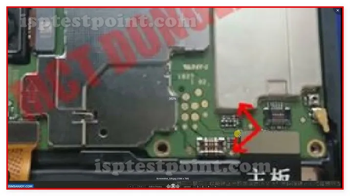
Locate the test pads on the mainboard, typically positioned near the eMMC memory chip on the rear or front side of the PCB. Power down the device completely and remove the back cover and battery (if removable). Use a magnifying glass or microscope to identify the small metallic contact pads. Connect your ISP tool (UMT, EasyJTAG Plus, or equivalent) to the designated test points using precise micro-probes or pogo-pin connectors. Establish a stable connection before initiating any read or write operation. Connect USB to the computer running your flashing software and proceed with the intended operation.
Common Test Point Locations
The primary test point cluster is located adjacent to the eMMC memory chip. Key measurement areas include CLK, CMD, DAT0-DAT7, VCC, GND, VCCQ, and RST pads. These points follow standard eMMC interface specifications. The exact coordinates and pad spacing require visual inspection under magnification due to component density variations across production batches. Reference the device's schematic diagram when available for precise pad identification.
Safety and Precautions
Always discharge static electricity before touching internal components. Verify tool voltage settings match the device's 1.8V/3.3V eMMC specifications to prevent electrical damage. Never apply probes while the device is powered or connected to USB without proper tool configuration. Ensure all connections are stable before initiating any operation. Improper probe contact or reversed polarity can permanently damage the eMMC or supporting circuitry. Perform a test read before any write operation to verify connectivity and data integrity. Keep detailed documentation of all operations performed for warranty and tracking purposes.
Pin / Test Point Reference
| Pin | Description |
|---|---|
| CLK | eMMC clock signal — 1.8V logic level |
| CMD | eMMC command/response line — Pull-up required |
| DAT0 | eMMC data line 0 — Primary data path |
| DAT1 | eMMC data line 1 |
| DAT2 | eMMC data line 2 |
| DAT3 | eMMC data line 3 |
| VCC | eMMC power supply 3.3V — Critical for device power |
| VCCQ | eMMC I/O voltage 1.8V |
| GND | Ground reference — Multiple pads present |
| RST | eMMC reset signal — Active low |
Tools required: UMT (Universal ModemTools), EasyJTAG Plus, Micro-probe set or pogo-pin connector, Magnifying glass/USB microscope, Multimeter for voltage verification, Anti-static wrist strap
Supported operations: Firmware Read (Full Flash), Firmware Write/Flashing, FRP Erase, Dead Boot Repair, IMEI Restoration, Bootloader Access, Partition-level repairs
⚠ Safety note: Device operates at 1.8V logic levels. Verify tool voltage configuration before connection. Risk of permanent eMMC/mainboard damage if improper voltage applied. Only qualified technicians should perform these operations. Disconnect power and USB before probe connection.

Comments (0)
Be the first to comment.